GaN-based heterojunction varactor device and epitaxial structure thereof
An epitaxial structure and heterojunction technology, applied in the field of varactors, can solve problems such as poor power characteristics, achieve high breakdown voltage, wide and flexible application design scenarios, and good thermal stability.
- Summary
- Abstract
- Description
- Claims
- Application Information
AI Technical Summary
Problems solved by technology
Method used
Image
Examples
Embodiment 1
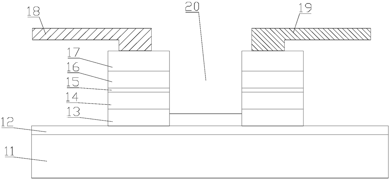
[0021] refer to figure 1 , a GaN-based heterojunction varactor device, including a substrate 11, a high-resistance buffer layer 12, a first heavily doped conductive layer 13, a first low-doped layer 14, and a wide bandgap from bottom to top The barrier layer 15, the second low-doped layer 16 and the second heavily-doped conductive layer 17; the first low-doped layer 14, the barrier layer 15 of the wide band gap and the second low-doped layer 16 to form a heterojunction barrier structure; the high-resistance buffer layer 12, the first layer of heavily doped conductive layer 13, the first layer of low-doped layer 14, the barrier layer 15 of a wide band gap, the second layer of low-doped Materials of the impurity layer 16 and the second heavily doped conductive layer 17 are both GaN-based materials.
[0022] The material of the substrate 11 is one of GaN, Si, sapphire and SiC, and the material of the substrate 11 is non-polar, semi-polar or polar. The thickness of the substrate...
Embodiment 2
[0028] refer to figure 1 , an epitaxial structure of a GaN-based heterojunction varactor device, comprising a metal anode 18, a metal cathode 19 and the GaN-based heterojunction varactor device described in Embodiment 1; between the metal anode 18 and the metal cathode 19 There is a groove 20 , and the bottom of the groove 20 is the first heavily doped conductive layer 13 .
[0029] Good ohmic contact is formed between the metal anode 18 and the metal cathode 19 and the second heavily doped conductive layer 17 .
[0030] The metal material of the metal anode 18 is one or more stacks in Ti, Al, Ni, Cr, Pt, Cu, Ag, Au, etc., but not limited to the above metal types; the metal material of the metal cathode 19 is Ti, Al, One or more stacks of Ni, Cr, Pt, Cu, Ag, Au, etc., but not limited to the above metal types. Both the thickness of the metal anode 18 and the thickness of the metal anode 19 are in the range of 50 nm-10 μm.
PUM
| Property | Measurement | Unit |
|---|---|---|
| Thickness | aaaaa | aaaaa |
| Thickness | aaaaa | aaaaa |
| Thickness | aaaaa | aaaaa |
Abstract
Description
Claims
Application Information
 - R&D
- Intellectual Property
- Life Sciences
- Materials
- Tech Scout
- Unparalleled Data Quality
- Higher Quality Content
- 60% Fewer Hallucinations
Browse by: Latest US Patents, China's latest patents, Technical Efficacy Thesaurus, Application Domain, Technology Topic, Popular Technical Reports.
© 2025 PatSnap. All rights reserved.Legal|Privacy policy|Modern Slavery Act Transparency Statement|Sitemap|About US| Contact US: help@patsnap.com


