A method of designing an integrated circuit with a porous dielectric layer

A technology of porous dielectric layer and integrated circuit, applied in computer-aided design, calculation, electrical digital data processing and other directions, can solve problems such as cost increase, pollution, danger, etc., to improve stability and reliability, reduce preparation process, Accurate and fast effect

Active Publication Date: 2022-04-22
深圳市恒凯微电子科技有限公司
View PDF0 Cites 0 Cited by
  • Summary
  • Abstract
  • Description
  • Claims
  • Application Information

AI Technical Summary

Problems solved by technology

[0004] However, the use of low-K or ultra-low-K insulating dielectric materials poses new requirements for semiconductor manufacturing processes. On the one hand, in order to obtain low-K materials or ultra-low-K materials and reduce the K value of materials, the materials usually used are porous materials. However, the mechanical strength of porous materials is relatively low, which leads to easy damage to the insulating dielectric layer during the process of etching through holes or trenches. On the other hand, the porous insulating dielectric layer is easily infiltrated by external materials, causing pollution , reducing the reliability of the material
Existing academic studies have pointed out that the "open" pore structure exposed to the outside when etching the porous dielectric layer can be formed into a closed structure through an additional "plugging" process, so as to prevent metal impurities from easily forming an interconnection structure. However, the additional process not only increases the cost, but also easily changes the shape of the through hole or trench formed by etching, resulting in the unsatisfactory effect of the final interconnection structure; and In the process of etching through holes or trenches, the opening of the mask layer will be used to further etch to form a through hole or trench structure. In order to increase the precise formation of the opening, the mask structure usually used is a double-layer mask structure. When forming the opening of the mask layer, it is necessary to use photoresist to define the position of the opening first, and then expose and develop the photoresist to form the opening.
[0005] In this case, before etching the insulating dielectric layer, a step of forming a multi-layer mask layer, a step of forming a photoresist, and then a step of exposing and developing, and after etching to form an opening, the remaining The photoresist and the remaining mask layer removal steps are cumbersome. At the same time, the developer commonly used in the photoresist development process is a mixed solution of methyl isobutyl ketone + isopropanol, and these organic substances are toxic. Substances, dangerous if inhaled, not conducive to safe production

Method used


Image

  • A method of designing an integrated circuit with a porous dielectric layer
  • A method of designing an integrated circuit with a porous dielectric layer
  • A method of designing an integrated circuit with a porous dielectric layer

Examples


Embodiment Construction

[0021] In the following description, the method for preparing the semiconductor interconnection structure proposed by the present invention will be further described in detail with reference to the accompanying drawings and examples, in order to provide a more thorough understanding of the present invention through specific details. It should be noted that all the drawings are in a very simplified form and use imprecise scales, and are only used to facilitate and clearly assist the purpose of illustrating the embodiments of the present invention. In the embodiments, in order to avoid confusion with the present invention, some technical features known in the art are not described.

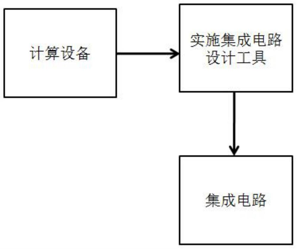
[0022] Please refer to the attached figure 1 The schematic diagram of the integrated circuit formed by the computing device is shown in the present invention, and the integrated circuit design tool is controlled by the computing device to control the integrated circuit to form the desired integrated...


PUM

PropertyMeasurementUnit
thicknessaaaaaaaaaa

Abstract

The present invention relates to a method for designing an integrated circuit with a porous dielectric layer. The method controls an integrated circuit design tool (femtosecond laser device) through a computing device. The method does not require the use of a mask process, thus eliminating the need for a reticle. It breaks through the limitation of the mask plate, does not use toxic developing steps, and also saves the "blocking" process of the exposed pore structure of the porous medium layer, reduces the preparation process, shortens the preparation process, saves costs, and The stability and reliability of the semiconductor device are improved.

Description

technical field [0001] A method for designing an integrated circuit with a porous dielectric layer by implementing an integrated circuit design tool on a computing device, in particular a method for forming an integrated circuit by using a femtosecond laser device to etch a porous dielectric layer. Background technique [0002] The rapid development of semiconductor integrated circuit technology constantly puts forward new requirements for the development of interconnection technology. At present, in the back-end process of semiconductor manufacturing, in order to connect the integrated circuits composed of various components, metal materials with relatively high conductivity are usually used, but as the size of semiconductor devices continues to shrink, the interconnection structure becomes narrower and narrower. , resulting in higher and higher interconnect resistances. [0003] In the existing process of forming copper wiring or copper interconnection, trenches or via ho...

Claims


Application Information

Patent Timeline
Patent Type & Authority Patents(China)
IPC IPC(8): G06F30/392
CPCG06F30/392
Inventor 赵红英
Owner 深圳市恒凯微电子科技有限公司
Why Eureka
Try Eureka