A method for preparing a semiconductor structure with a porous dielectric layer

A porous dielectric layer and semiconductor technology, which is applied in semiconductor/solid-state device manufacturing, semiconductor devices, semiconductor/solid-state device components, etc. Solve problems such as changes in groove shape, achieve fast and accurate etching, and shorten the etching time

Active Publication Date: 2020-09-18
XINYI XIYI ADVANCED MATERIALS RES INST OF IND TECH CO LTD
View PDF4 Cites 0 Cited by
  • Summary
  • Abstract
  • Description
  • Claims
  • Application Information

AI Technical Summary

Problems solved by technology

[0004] However, the use of low-K or ultra-low-K insulating dielectric materials poses new requirements for semiconductor manufacturing processes. On the one hand, in order to obtain low-K materials or ultra-low-K materials and reduce the K value of materials, the materials usually used are porous materials. However, the mechanical strength of porous materials is relatively low, which leads to easy damage to the insulating dielectric layer during the process of etching through holes or trenches. On the other hand, the porous insulating dielectric layer is easily infiltrated by external materials, causing pollution , reducing the reliability of the material
Existing academic studies have pointed out that the "open" pore structure exposed to the outside when etching the porous dielectric layer can be formed into a closed structure through an additional "plugging" process, so as to prevent metal impurities from easily forming an interconnection structure. However, the additional process not only increases the cost, but also easily changes the shape of the through hole or trench formed by etching, resulting in a less than ideal effect of the final interconnection structure; and usually Next, there are other interconnection structures under the through holes or trenches formed in the interlayer dielectric layer. During etching, it is easy to cause damage to the underlying interconnection structure, which will affect the stability and reliability of semiconductor devices. Sex makes a big difference

Method used


Image

  • A method for preparing a semiconductor structure with a porous dielectric layer
  • A method for preparing a semiconductor structure with a porous dielectric layer
  • A method for preparing a semiconductor structure with a porous dielectric layer

Examples


Embodiment Construction

[0025] In the following description, the method for preparing the semiconductor interconnection structure proposed by the present invention will be further described in detail with reference to the accompanying drawings and examples, in order to provide a more thorough understanding of the present invention through specific details. It should be noted that all the drawings are in a very simplified form and use imprecise scales, and are only used to facilitate and clearly assist the purpose of illustrating the embodiments of the present invention. In the embodiments, in order to avoid confusion with the present invention, some technical features known in the art are not described.

[0026] Please refer to the attached figure 1 The schematic diagram of the preparation process of the present invention shown, the preparation method includes the following process steps:

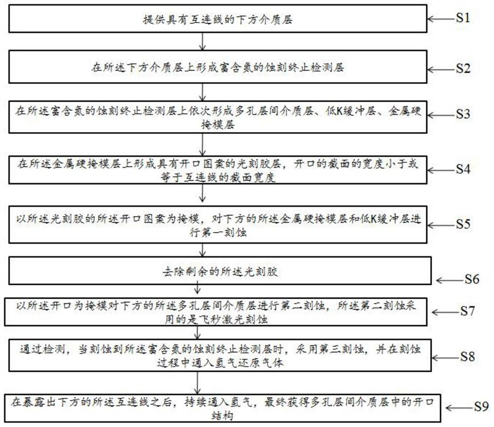
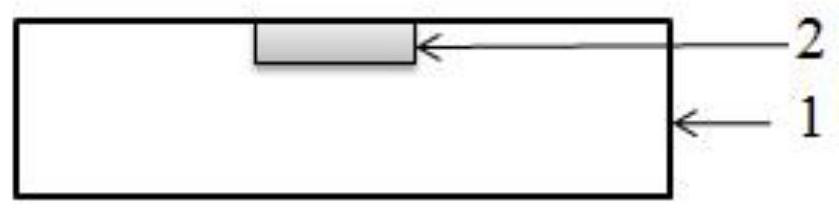
[0027] Step S1: providing a lower dielectric layer with interconnection lines;

[0028] Step S2: forming a ni...


PUM

PropertyMeasurementUnit
thicknessaaaaaaaaaa
thicknessaaaaaaaaaa
thicknessaaaaaaaaaa

Abstract

The invention provides a method of preparing a semiconductor structure having a porous dielectric layer. The method comprises: a lower dielectric layer having interconnect lines is provided; a nitrogen-rich etch stop detection layer, a porous inter-layer dielectric layer, a low-k buffer layer, a metal hard mask layer, and a photoresist layer with an opening pattern are formed on the lower dielectric layer successively; first etching is carried out on the metal hard mask layer and the low-k buffer layer below by using the opening pattern of the photoresist as a mask; the rest of photoresist isremoved; second etching is carried out on the porous inter-layer dielectric layer below by using the opening as a mask, wherein the second etching employs femtosecond laser etching and the edge of theexposed hole structure is melted partially to seal the exposed hole structure when the porous inter-layer dielectric layer is etched by using femtosecond laser; third etching is carried out and hydrogen gas is introduced during the etching; and after exposure of the lower interconnect lines, hydrogen gas is continuously led to obtain an open structure in the porous inter-layer dielectric layer.

Description

technical field [0001] The invention relates to a method for preparing a semiconductor structure, in particular to a method for preparing a semiconductor structure with a porous low-K or ultra-low-K interlayer dielectric layer. Background technique [0002] The rapid development of semiconductor integrated circuit technology constantly puts forward new requirements for the development of interconnection technology. At present, in the back-end process of semiconductor manufacturing, in order to connect the integrated circuits composed of various components, metal materials with relatively high conductivity are usually used, but as the size of semiconductor devices continues to shrink, the interconnection structure becomes narrower and narrower. , resulting in higher and higher interconnect resistances. With the help of copper's excellent electrical conductivity, copper interconnection technology has been widely used in the technology of 90nm and 65nm technology nodes. [00...

Claims


Application Information

Patent Timeline
Patent Type & Authority Patents(China)
IPC IPC(8): H01L21/768H01L21/311H01L23/532
CPCH01L21/31127H01L21/31138H01L21/76802H01L21/7682H01L21/76838H01L23/5329H01L2221/1047
Inventor 赵红英
Owner XINYI XIYI ADVANCED MATERIALS RES INST OF IND TECH CO LTD
Why Eureka
Try Eureka