Preparation method of flexible printed circuit board

A flexible printing and circuit board technology, applied in printed circuit manufacturing, laminated printed circuit boards, printed circuits, etc., can solve problems such as defective flexible printed circuit boards, improve the flatness of the board surface, and reduce the height difference , reduce the effect of open circuit

Inactive Publication Date: 2018-08-10
深圳市爱升精密电路科技有限公司
View PDF3 Cites 0 Cited by
  • Summary
  • Abstract
  • Description
  • Claims
  • Application Information

AI Technical Summary

Problems solved by technology

[0003] The invention provides a method for preparing a flexible printed circuit board, aiming at the problem that the existing substrate has a stepped structure that easily leads to defective flexible printed circuit boards.

Method used


Image

  • Preparation method of flexible printed circuit board

Examples


Embodiment Construction

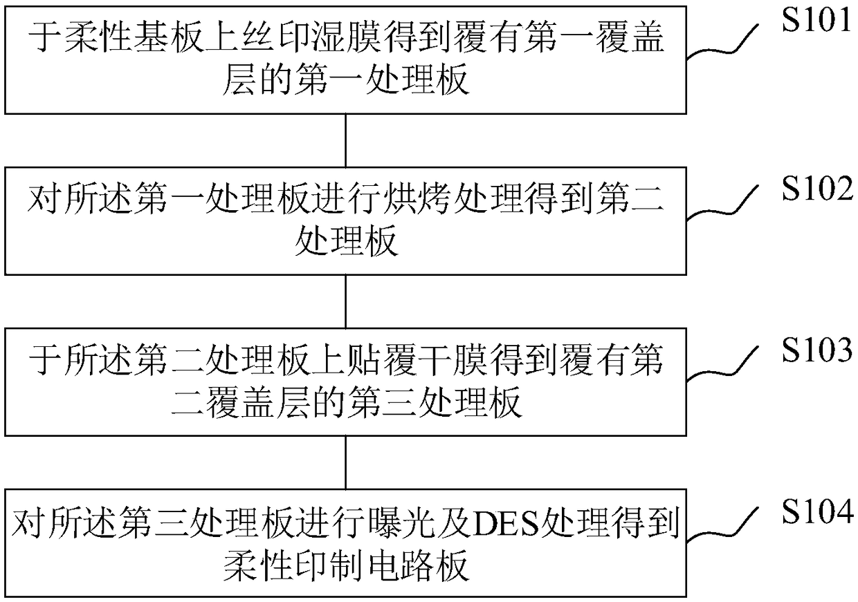
[0020] In order to make the object, technical solution and advantages of the present invention clearer, the implementation manner of the present invention will be further described in detail below in conjunction with the accompanying drawings.

[0021] The processing of printed circuit boards in the way of selective copper plating can meet the flexible requirements of contemporary printed circuit boards, aiming at the step structure formed when the copper plating area and the non-copper plating area connected to the copper plating area have a height difference , especially when the height difference is greater than or equal to 40 microns, the printed circuit board prepared according to the traditional process may cause a short circuit caused by poor exposure during the exposure stage due to the height difference. Leading to problems such as scrapping, the present invention provides a method for preparing a flexible printed circuit board to solve or partially solve the above pro...


PUM


Abstract

The invention discloses a preparation method of a flexible printed circuit board, and relates to a preparation process of the printed circuit board. The preparation method of the flexible printed circuit board comprises the steps of carrying out the screen printing of a wet film on a flexible substrate to obtain a first processing board covered with a first covering layer; carrying out baking treatment on the first processing board to obtain a second processing board; coating a dry film on the second processing board to obtain a third processing board covered with a second covering layer; carrying out exposure and DES treatment on the third processing board to obtain the flexible printed circuit board. By means of the method and the device, the probability of poor flexibility of the flexible printed circuit board due to the fact that the step structure of the flexible substrate is prone to being caused can be reduced.

Description

technical field [0001] The invention relates to a preparation process of a printed circuit board, in particular to a preparation method of a flexible printed circuit board. Background technique [0002] In the current market, in order to meet the flexible requirements of electronic products, selective copper plating is used in the printed circuit board preparation process to process the circuit board. The result of this treatment is the connection position between the copper-plated area and the non-copper-plated area. There will be a ladder structure. When processing printed circuit boards using the general wet film method, if the height difference of the stepped structure is more than 40 microns, after the conventional 50 micron dry film is wet pasted, it is easy to appear in the stepped structure because it cannot be filled. Bubbles, and the appearance of bubbles will cause the dry film to be unable to adhere closely to the copper surface, and it is easy to cause a short ...

Claims


Application Information

Patent Timeline
Patent Type & Authority Applications(China)
IPC IPC(8): H05K3/00
CPCH05K3/0058
Inventor 陈福巧
Owner 深圳市爱升精密电路科技有限公司
Why Eureka
Try Eureka