Flexible LED package

A technology of LED encapsulation and flexible type, which is applied in the direction of electrical components, circuits, semiconductor devices, etc., can solve the problems of LED light source loss, etc., and achieve the effects of prolonging the service life, simplifying the manufacturing method, and reducing the manufacturing cost

Inactive Publication Date: 2018-08-17
陈慧仪
View PDF0 Cites 0 Cited by
  • Summary
  • Abstract
  • Description
  • Claims
  • Application Information

AI Technical Summary

Problems solved by technology

[0004] However, the LED light source will still be lost during the reflection process, and cause different degrees of light loss according to the length or angle of the reflection path, and can only achieve the effect of single-sided light emission

Method used


Image

  • Flexible LED package
  • Flexible LED package
  • Flexible LED package

Examples


Embodiment 1

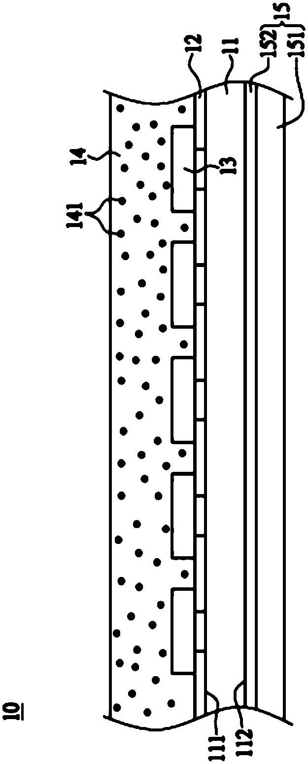
[0024] see figure 1 , is a schematic cross-sectional view of a flexible LED package 10 according to Embodiment 1 of the present invention. The flexible LED package 10 of this embodiment includes a flexible light-transmitting substrate 11, a bendable circuit layer 12, and at least one light-emitting diode 13. A flexible transparent cover 14 and a fluorescent patch 15 .

[0025] Specifically, the flexible transparent substrate 11 is made of a material with high light transmission and flexibility, such as polyethylene terephthalate (PET), polyethylene naphthalate (PEN), polyethylene Imide (PI), polymethylmethacrylate (PMMA) or polyethersulfone (PES), etc., but not limited thereto. In this embodiment, the flexible light-transmitting substrate 11 has an upper surface 111 and a lower surface 112 with a thickness of 0.01-1 mm.

[0026] The bendable circuit layer 12 is formed on the upper surface 111 of the flexible light-transmitting substrate 11 by printing, sputtering, etc., of a...

Embodiment 2

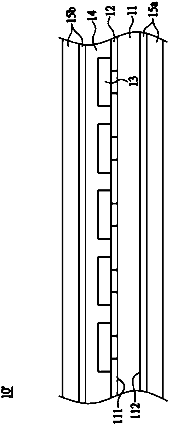
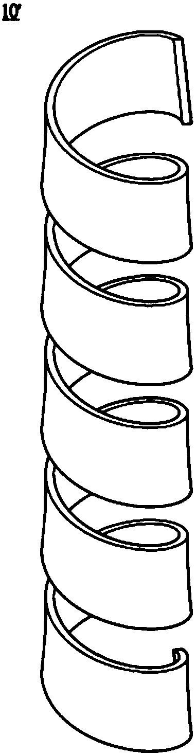
[0035] see figure 2, is a schematic cross-sectional view of a flexible LED package 10' in Embodiment 2 of the present invention. The difference from Embodiment 1 is that the flexible light-transmitting cover 14 of the flexible LED package in this embodiment may not include fluorescent light. The powder 141 is further covered on the flexible transparent cover 14 with another fluorescent patch 15 .

[0036] Specifically, in this embodiment, the flexible LED package includes a flexible light-transmitting substrate 11, a bendable circuit layer 12, at least one light-emitting diode 13, a flexible light-transmitting cover 14 and at least A fluorescent patch 15 . Among them, the number of fluorescent patches 15 is two, the first fluorescent patch 153 covers the lower surface 112 of the flexible transparent substrate 11, and the second fluorescent patch 154 covers the flexible transparent cover. 14, so as to achieve the effect of double-sided light emission.

[0037] It is worth n...


PUM


Abstract

Flexible LED package comprises a flexible transmitting substrate, a bendable circuit layer, at least one light-emitting diode, a flexible transmitting cover and at least one fluorescent patch, whereinthe flexible transmitting substrate is provided with an upper surface and a lower surface, the bendable circuit layer is arranged on the upper surface of the flexible transmitting substrate, the light-emitting diode is arranged on the upper surface of the flexible transmitting substrate and is electrically connected to the bendable circuit layer, the flexible transmitting cover is arranged on theupper surface of the flexible transmitting substrate and covers the light-emitting diode and the bendable circuit layer, and the fluorescent patch covers one of lower surfaces of the flexible transmitting cover and the flexible transmitting substrate. Therefore, by the flexible LED package, the effect of uniform light emitting from two surfaces can be achieved.

Description

technical field [0001] The invention relates to an LED package structure, in particular to a flexible LED package capable of emitting light from both sides. Background technique [0002] Light-emitting diode (Light-EmittingDiode, LED) has the advantages of small size, low power consumption, high brightness, high color performance, fast response, and can be used continuously for 20,000 to 50,000 hours. It is in line with energy-saving and environmentally friendly green lighting Therefore, solid-state light source (SSL) systems such as traditional fluorescent lamps and light bulbs are gradually replaced, and are widely used in electronic products, display device backlights, indicator lights, mobile communications and other fields. [0003] Generally speaking, in order to improve the luminous efficiency of the traditional LED package structure, a reflective layer is usually arranged on one side of the LED package structure, and a light-transmitting substrate is arranged on the ...

Claims


Application Information

Patent Timeline
Patent Type & Authority Applications(China)
IPC IPC(8): H01L33/48H01L33/58
CPCH01L33/48H01L33/58
Inventor 陈慧仪
Owner 陈慧仪
Why Eureka
Try Eureka