Awaking method and device of FPGA (Field Programmable Gate Array) chip

A chip and wake-up circuit technology, applied to program control devices, program control design, instruments, etc., can solve the problems of system power failure, FPGA chip cannot be processed, FPGA chip cannot be woken up from standby, etc.

Active Publication Date: 2018-08-24
BOE TECH GRP CO LTD
View PDF5 Cites 5 Cited by
  • Summary
  • Abstract
  • Description
  • Claims
  • Application Information

AI Technical Summary

Problems solved by technology

[0003] At present, during the use of FPGA chips, because they are used in large-scale integrated circuits, and the power supply for them is the whole system power supply, so when standby is required, the entire system is usually powered off, and in this case In this case, when the standby state needs to be released, or the external signal with the FPGA interface is hot-swapped, the FPGA chip cannot process it.
[0004] Therefore, there is a technical problem in the prior art that the FPGA chip cannot be woken up from standby

Method used


Image

  • Awaking method and device of FPGA (Field Programmable Gate Array) chip
  • Awaking method and device of FPGA (Field Programmable Gate Array) chip
  • Awaking method and device of FPGA (Field Programmable Gate Array) chip

Examples


Embodiment Construction

[0032] The following will clearly and completely describe the technical solutions in the embodiments of the present invention with reference to the drawings in the embodiments of the present invention.

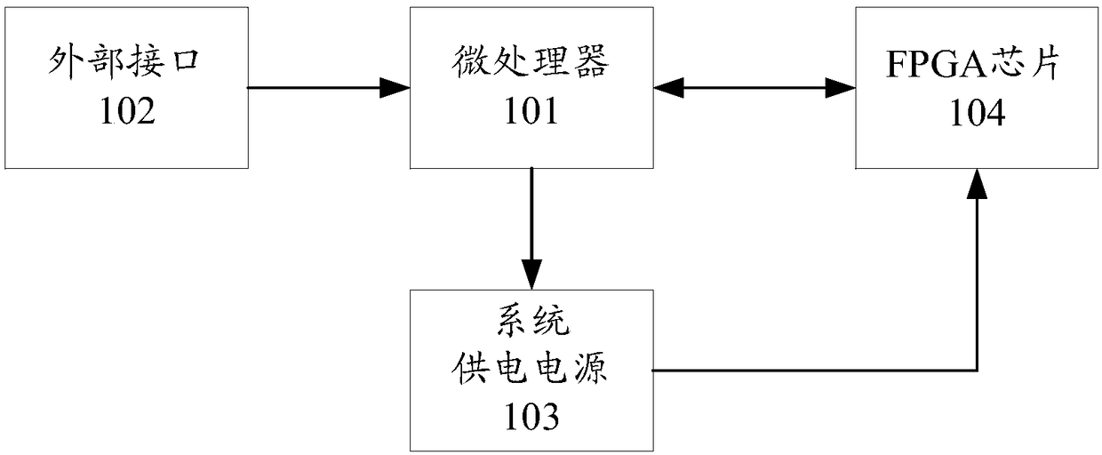
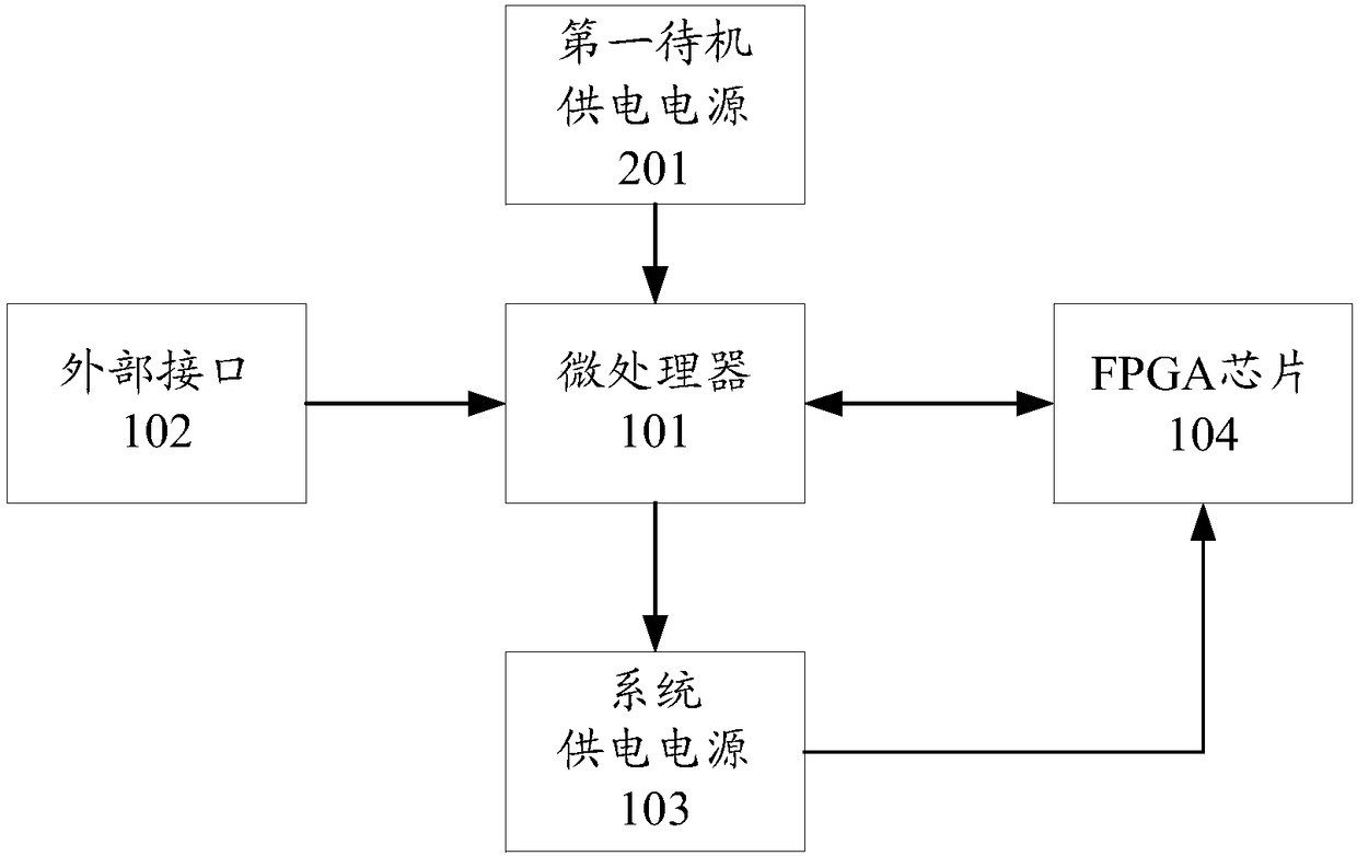
[0033] An embodiment of the present invention provides a wake-up circuit for an FPGA chip. The wake-up circuit can be applied to an electronic device including an FPGA chip, such as a display, a TV, a notebook computer, a smart phone, a smart watch, a tablet computer, and the like.

[0034] figure 1 It is a structural representation of the wake-up circuit of the FPGA chip in the embodiment of the present invention Figure 1 , see figure 1 As shown, the wake-up circuit of the FPGA chip can include: a microprocessor 101, an external interface 102, a system power supply 103 and an FPGA chip 104;

[0035]Wherein, the external interface is configured to output the external access signal from the external signal source to the microprocessor; the microprocessor is configured to det...


PUM


Abstract

The invention provides an awaking circuit and method of an FPGA (Field Programmable Gate Array) chip for realizing an effect that the FPGA chip in a standby state can be awoken by an external input signal. The circuit includes: a microprocessor, an external interface, a system power supply and the FPGA chip. The external interface is configured for outputting an external access signal from an external signal source to the microprocessor. The microprocessor is configured for detecting whether the external input signal meets an awaking condition; and outputting a power supply signal to the system power supply when the external input signal meeting the awaking condition is detected. The system power supply is configured for receiving and responding to the power supply signal from the microprocessor, and supplying power to the FPGA chip to awake the FPGA chip.

Description

technical field [0001] The invention relates to the field of field programmable gate array (FPGA, Field Programmable Gate Array) design, in particular to a method and device for waking up an FPGA chip. Background technique [0002] FPGA chips, that is, field programmable gate array chips, are used in programmable array logic (PAL, Programmable Array Logic), general array logic (GAL, Generic Array Logic), complex programmable logic devices (CPLD, Complex Programmable Logic Device), etc. The product of further development on the basis of programmable devices. It emerged as a semi-custom circuit in the field of ASIC (Application Specific Integrated Circuit), which not only solves the shortcomings of custom circuits, but also overcomes the shortcomings of the limited number of original programmable device gates. [0003] At present, during the use of FPGA chips, since they are used in large-scale integrated circuits, and the power supply for them is the whole system power suppl...

Claims


Application Information

Patent Timeline
Patent Type & Authority Applications(China)
IPC IPC(8): G06F9/4401
CPCG06F9/4418
Inventor 王红王永波
Owner BOE TECH GRP CO LTD
Why Eureka
Try Eureka