Nitride light emitting diode assembly
A technology of light-emitting diodes and nitrides, applied in electrical components, semiconductor devices, circuits, etc., can solve the problems of uncontrollable opening size and defect density, uneven distribution of electronic holes in LED devices, and affecting LED luminous efficiency. Achieve the effects of improving hole injection efficiency, reducing electron migration rate, and improving effective recombination radiation luminous efficiency
- Summary
- Abstract
- Description
- Claims
- Application Information
AI Technical Summary
Problems solved by technology
Method used
Image

Examples
Embodiment 1
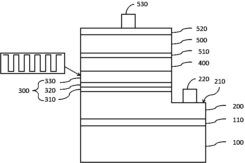
[0027] figure 1 It is a schematic cross-sectional view of a nitride light-emitting diode assembly proposed in this embodiment. See attached figure 1 Firstly, a substrate 100 is provided, and the material of the substrate 100 can be sapphire, silicon, silicon carbide, zinc oxide, gallium nitride, aluminum nitride or other materials suitable for crystal epitaxial growth. Next, an N-type doped nitride layer 200 is formed on the upper surface of the substrate 100. The material of the N-type doped nitride layer 200 can be GaN doped with silicon or germanium or tin or lead, and can also contain unintentionally doped GaN layer. In this embodiment, the N-type doped nitride layer 200 has a platform 210 on which a first electrode 220 is formed.
[0028] Before forming the N-type doped nitride, a step of forming a buffer layer 110 on the substrate 100 is also included. The buffer layer 110 can improve the problem of the lattice constant mismatch between the N-type doped nitride layer...
Embodiment 2
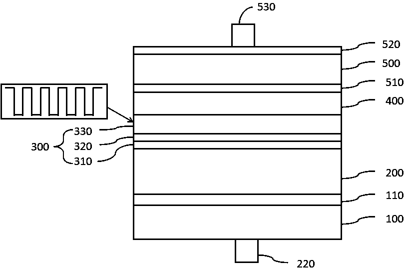
[0045] The difference between this embodiment and Embodiment 1 is that the third defect regulating layer 330 has a single-layer structure, which can be a single-layer structure of aluminum-containing ternary nitride, such as an AlGaN single-layer or an InAlN single-layer; it can also be an aluminum-containing quaternary nitride Nitride monolayer structure, such as AlInGaN monolayer.
[0046] See attached Figure 4 A nitride light-emitting diode assembly provided in this embodiment includes a substrate 100, and a buffer layer 110, an N-type doped nitride layer 200, a defect control layer 300, an active layer 400, The electron blocking layer 510 , the P-type doped nitride layer 500 and the P-type ohmic contact layer 520 . The N-type doped nitride layer 200 is provided with a platform 210 , a first electrode 220 is provided on the platform, and a second electrode 530 is located on the P-type ohmic contact layer 520 . The defect control layer 300 includes a first defect control ...
PUM
 Abstract
Description
Claims
Application Information
 - R&D Engineer
- R&D Manager
- IP Professional
- Industry Leading Data Capabilities
- Powerful AI technology
- Patent DNA Extraction
Browse by: Latest US Patents, China's latest patents, Technical Efficacy Thesaurus, Application Domain, Technology Topic.
© 2024 PatSnap. All rights reserved.Legal|Privacy policy|Modern Slavery Act Transparency Statement|Sitemap