Miniature RF and microwave components and methods for fabricating such components

a technology of miniature rf and microwave components, applied in the field of electric devices, can solve the problems of destructive separation of masking materials from substrates, and achieve the effect of reducing siz

Inactive Publication Date: 2007-08-21
MEMGEN CORP
View PDF91 Cites 108 Cited by
  • Summary
  • Abstract
  • Description
  • Claims
  • Application Information

AI Technical Summary

Benefits of technology

[0033]An object of various aspects of the invention is to provide RF components having reduced size.
[0034]An object of various aspects of the invention is to provide RF components producible with decreased manufacturing cost.
[0035]An object of various aspects of the invention is to provide RF components with enhanced reliability.
[0037]An object of various aspects of the invention is to provide RF components with features that provide enhanced capability, such as greater bandwidth.

Problems solved by technology

The CC mask plating process is distinct from a “through-mask” plating process in that in a through mask plating process the separation of the masking material from the substrate would occur destructively.

Method used


Image

  • Miniature RF and microwave components and methods for fabricating such components
  • Miniature RF and microwave components and methods for fabricating such components
  • Miniature RF and microwave components and methods for fabricating such components

Examples


Embodiment Construction

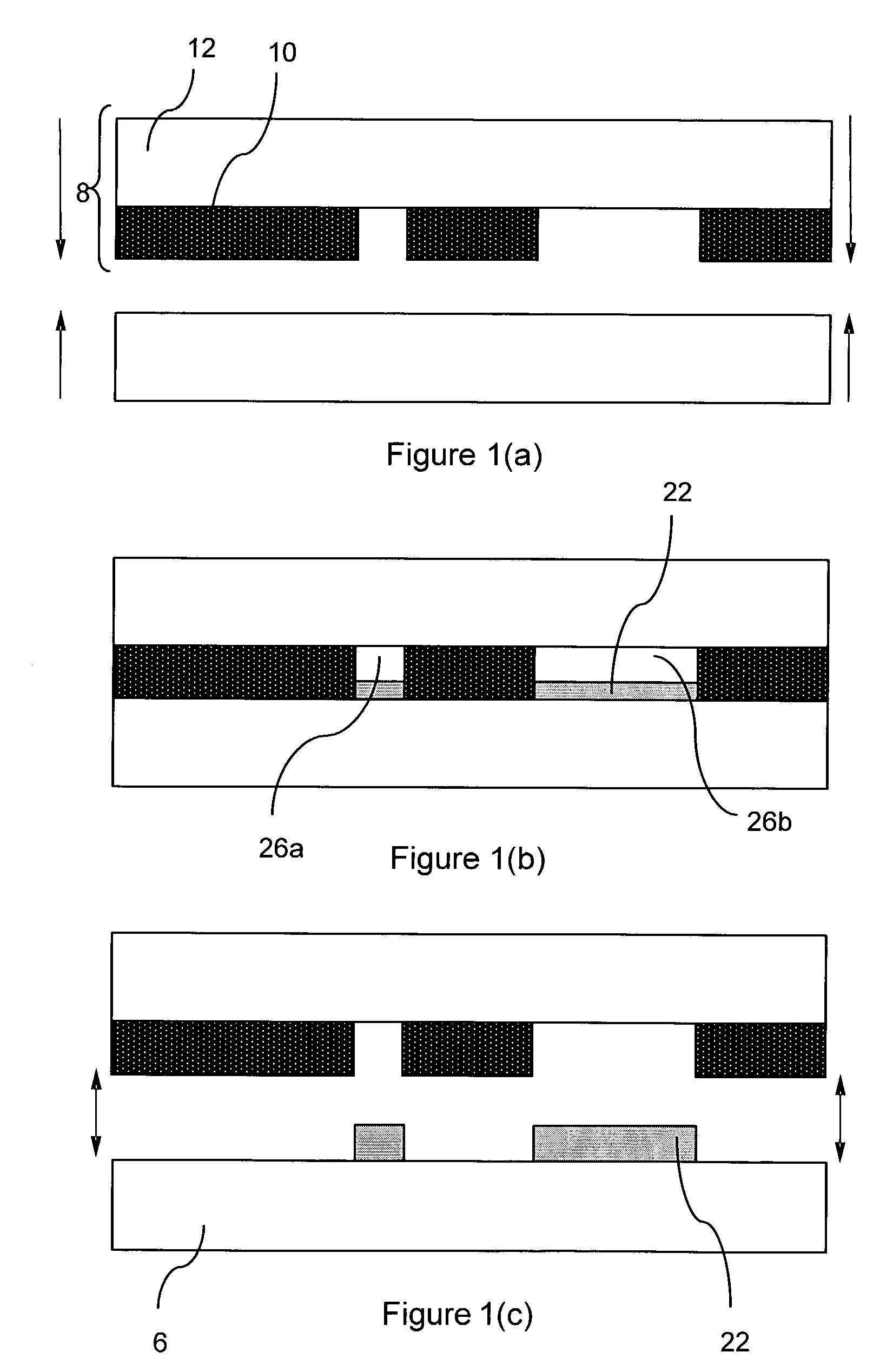
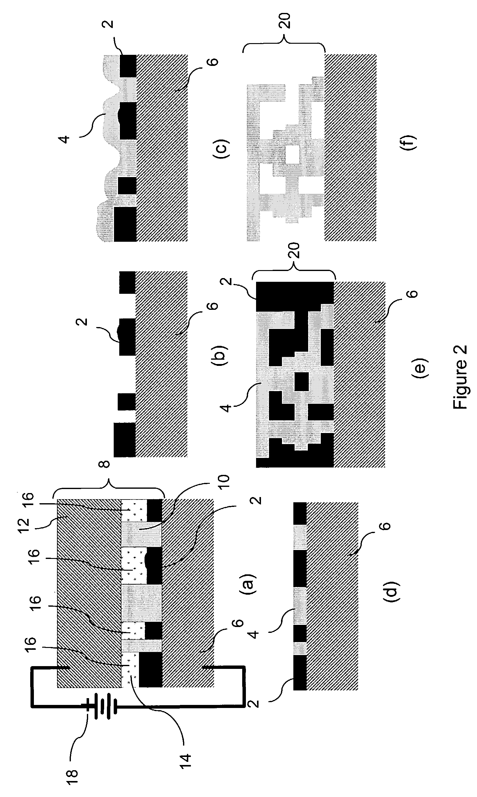
[0102]A basic process of electrochemically forming layers of multilayer three-dimensional structures was presented in FIGS. 1(a)-1(c), while FIGS. 2(a)-2(f) applied the layer forming technique to a plurality of overlaid layers (i.e. face-to-face contacting of layers regardless of whether successive layers are formed above, below, or beside previously formed layers). Various possible apparatus components were discussed with the aid of FIGS. 3(a)-3(c). This apparatus and these processes may be used in forming structures according to some embodiments of the invention. Other apparatus and processes may also be used.

[0103]For example, in some embodiments process variations may be used to yield cavities within the conductive structures that are filled completely or partially with a dielectric material, a conductive material embedded in a dielectric, or a magnetic material (e.g. a powdered ferrite material embedded in a dielectric binder or sintered after placement). The dielectric materia...


PUM

PropertyMeasurementUnit
frequencyaaaaaaaaaa
frequencyaaaaaaaaaa
frequencyaaaaaaaaaa

Abstract

RF and microwave radiation directing or controlling components are provided that may be monolithic, that may be formed from a plurality of electrodeposition operations and / or from a plurality of deposited layers of material, that may include switches, inductors, antennae, transmission lines, filters, and / or other active or passive components. Components may include non-radiation-entry and non-radiation-exit channels that are useful in separating sacrificial materials from structural materials. Preferred formation processes use electrochemical fabrication techniques (e.g. including selective depositions, bulk depositions, etching operations and planarization operations) and post-deposition processes (e.g. selective etching operations and / or back filling operations).

Description

RELATED APPLICATIONS[0001]This application claims priority to U.S. Provisional Patent Application Nos.: 60 / 338,638 filed on Dec. 3, 2001; 60 / 340,372 filed on Dec. 6, 2001; 60 / 379,133 filed on May 7, 2002; 60 / 379,182 filed on May 7, 2002; 60 / 379,184 filed on May 7, 2002; 60 / 415,374 filed on Oct. 1, 2002; 60 / 379,130 filed on May 7, 2002 and 60 / 392,531 filed on Jun. 27, 2002, all of which are incorporated herein by reference as if set forth in full.FIELD OF THE INVENTION[0002]Embodiments of this invention relate to the field of electrical devices and their manufacture while specific embodiments relate to RF and microwave devices and their manufacture. More particularly embodiments of this invention relate to miniature passive RF and microwave devices (e.g. filters, transmission lines, delay lines, and the like) which may be manufactured using, at least in part, a multi-layer electrodeposition technique known as Electrochemical Fabrication.BACKGROUND OF THE INVENTION[0003]A technique fo...

Claims


Application Information

Patent Timeline
Patent Type & Authority Patents(United States)
IPC IPC(8): H01P3/06H01P3/00B81B3/00G01P15/08G01P15/125H01P1/202H01P5/18H01P11/00H05K3/46
CPCG01P15/0802G01P15/125H01P1/202H01P3/06H01P5/183H01P11/005H01P11/007C25D1/003H01P11/00B81B2201/042Y10T29/49018H05K3/4647Y10T29/49016Y10T29/49002B33Y10/00
Inventor BROWN, ELLIOTT R.EVANS, JOHN D.BANG, CHRISTOPHER A.COHEN, ADAM L.LOCKARD, MICHAEL S.SMALLEY, DENNIS R.GROSSER, MORTON
Owner MEMGEN CORP
Why Eureka
Try Eureka