Array substrate and preparation method thereof and display device

A technology of array substrates and substrate substrates, applied in the direction of electrical components, electric solid devices, circuits, etc., can solve the problems of reduced storage capacitor area and difficult to meet the capacitance value of storage capacitors, so as to increase capacitance, meet design requirements, The effect of expanding the effective frontal area

A technology of array substrates and substrate substrates, applied in the direction of electrical components, electric solid devices, circuits, etc., can solve the problems of reduced storage capacitor area and difficult to meet the capacitance value of storage capacitors, so as to increase capacitance, meet design requirements, The effect of expanding the effective frontal area

CN108461529AInactive Publication Date: 2018-08-28BOE TECH GRP CO LTD

Image

  • Array substrate and preparation method thereof and display device
  • Array substrate and preparation method thereof and display device
  • Array substrate and preparation method thereof and display device

Examples


Embodiment Construction

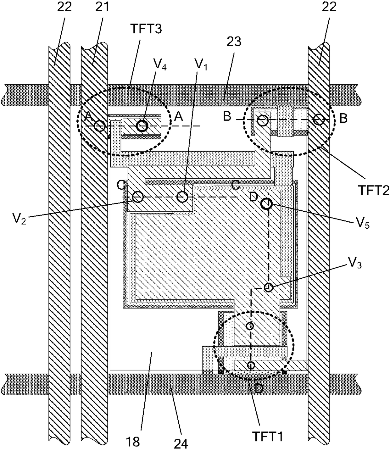
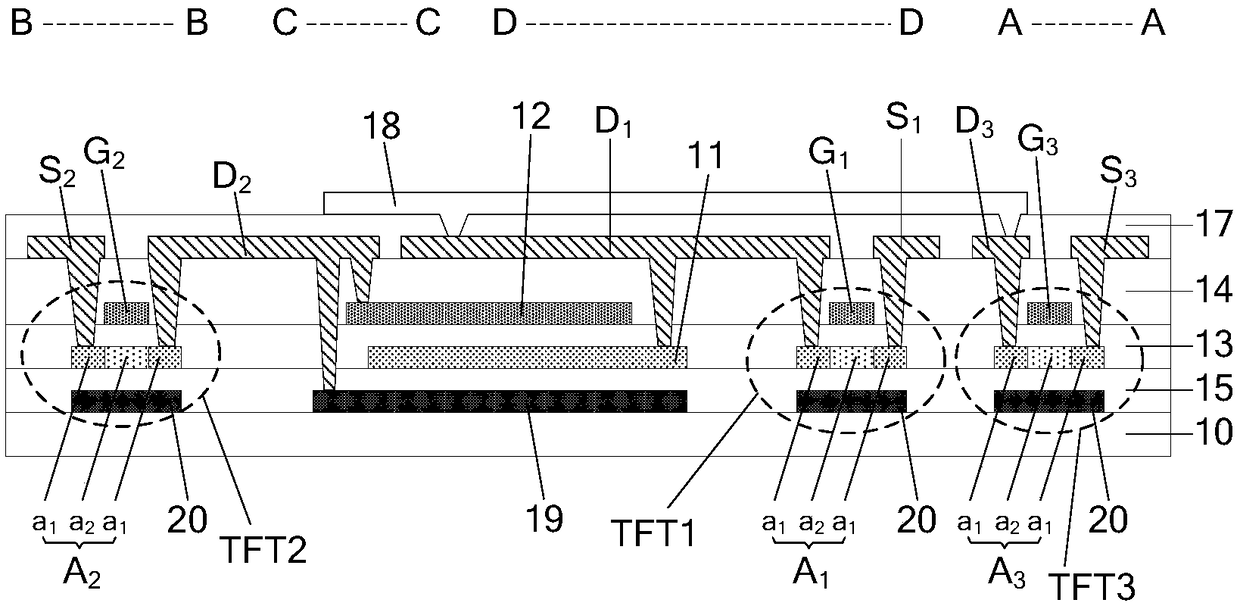
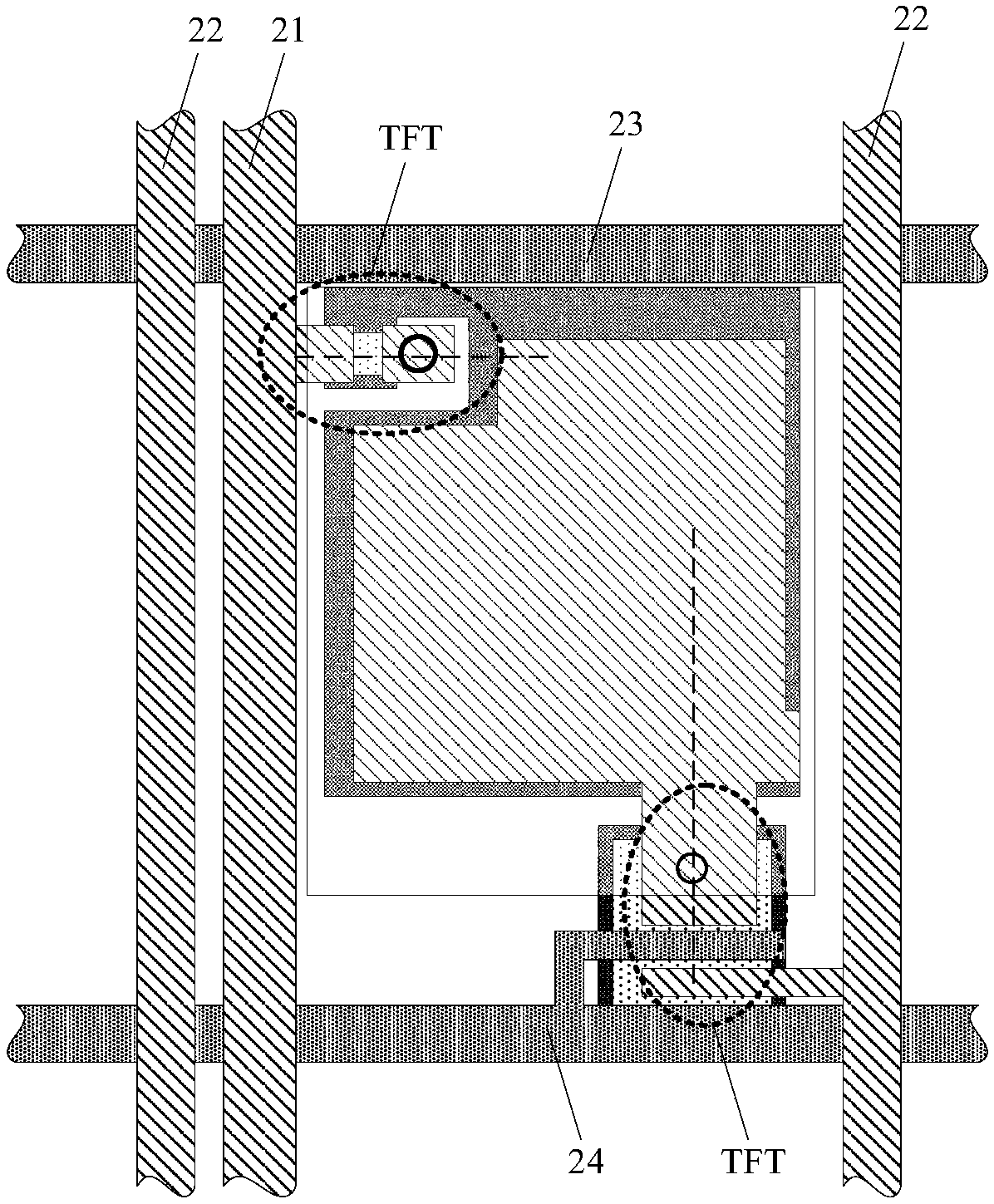
[0035] The following will clearly and completely describe the technical solutions in the embodiments of the present invention with reference to the accompanying drawings in the embodiments of the present invention. Obviously, the described embodiments are only some, not all, embodiments of the present invention. Based on the embodiments of the present invention, all other embodiments obtained by persons of ordinary skill in the art without making creative efforts belong to the protection scope of the present invention.

[0036]As an example, the terms "first", "second" and similar words used in the patent application specification and claims of the present invention do not indicate any order, quantity or importance, but are only used to distinguish different components . "Comprising" or "comprising" and similar words mean that the elements or items appearing before the word include the elements or items listed after the word and their equivalents, without excluding other eleme...


PUM


Abstract

The embodiment of the invention provides an array substrate and a preparation method thereof and a display device, and relates to the technical field of display. The capacitance of a capacitor can beincreased in a limited driving circuit arrangement area to meet the display requirement of high PPI. The array substrate comprises multiple pixel units arranged on a substrate; and each pixel unit comprises a first thin film transistor which comprises a first active pattern, a first source electrode, a first drain electrode and a first grid electrode, a first electrode and a second electrode, wherein the first grid electrode is located on the side, far away from the substrate, of the first active pattern, the first source electrode and the first drain electrode are located on the side, far away from the substrate, of the first grid and connected with the first active pattern through different via holes respectively, the first electrode and the first active pattern are arranged in the samelayer, the second electrode and the first grid electrode are arranged in the same layer, the first electrode is connected with the first drain electrode, and orthographic projections of any two of thefirst electrode, the second electrode and the first drain electrode on the substrate have an overlapping area.

Description

technical field [0001] The present invention relates to the field of display technology, in particular to an array substrate, a preparation method thereof, and a display device. Background technique [0002] In order to achieve a better picture display effect, the size of a single pixel unit (Pixel) in a display device is continuously reduced. A plurality of thin film transistors (Thin Film Transistor, TFT) usually arranged in the pixel unit occupies a large area in the pixel unit, and the arrangement area for the storage capacitor is too small, resulting in a reduction in the area of ​​the storage capacitor, resulting in the capacitance of the storage capacitor The problem that the value is difficult to meet the display requirements of high PPI (pixels per inch, the number of pixel units per inch). Contents of the invention [0003] In view of this, in order to solve the problems of the prior art, the embodiments of the present invention provide an array substrate and it...

Claims


Application Information

Patent Timeline
28 Aug 2018
Publication
CN108461529A
IPC
H01L27/32
CPC
H10K59/12; H10K59/1213; H10K59/1216; H10K59/126
Inventors
冯京; 尹东升