Light emitting diode epitaxial wafer and manufacturing method thereof
A technology of light-emitting diodes and manufacturing methods, which is applied to electrical components, circuits, semiconductor devices, etc., can solve the problems of low internal quantum luminous efficiency and external quantum luminous efficiency of LEDs, reduce polarization and stress, reduce thickness, The effect of improving the internal quantum luminous efficiency
- Summary
- Abstract
- Description
- Claims
- Application Information
AI Technical Summary
Problems solved by technology
Method used
Image

Examples
Embodiment 1
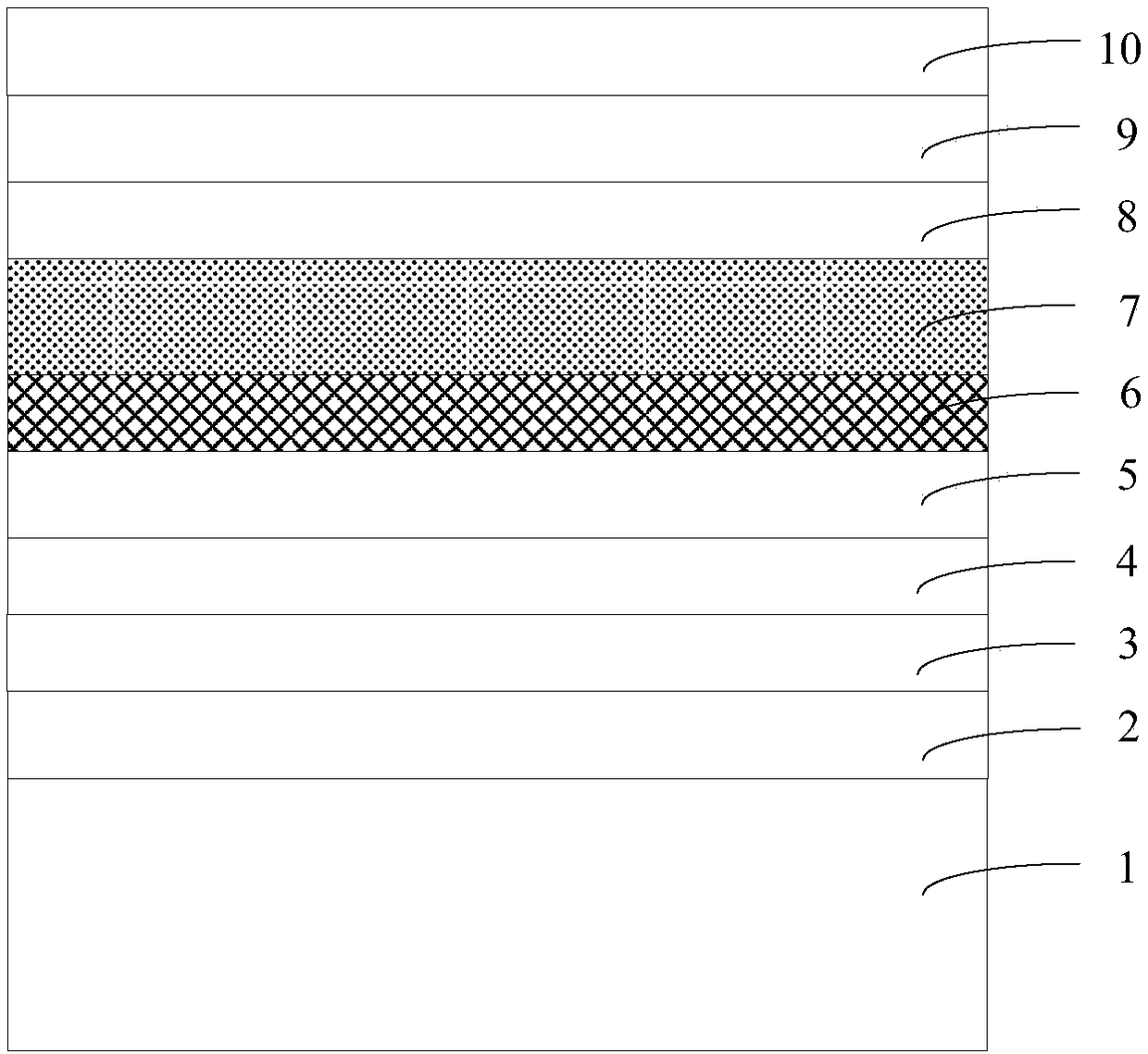
[0027] An embodiment of the present invention provides a light emitting diode, figure 1 It is a schematic structural diagram of a light-emitting diode epitaxial wafer provided by an embodiment of the present invention, as shown in figure 1 As shown, the light-emitting diode includes a substrate 1, a buffer layer 2, an undoped GaN layer 3, an N-type layer 4, a multi-quantum well layer 5, an insertion layer 6, and a low-temperature P-type layer stacked on the substrate 1 in sequence. layer 7, electron blocking layer 8, high temperature P-type layer 9, and P-type contact layer 10.
[0028] The low-temperature P-type layer 7 is a Mg-doped AlGaN / GaN superlattice structure or a Mg-doped AlGaN / InGaN superlattice structure, and the doping concentration of Mg in the low-temperature P-type layer 7 is greater than or equal to 1*10 20 cm -3 . The insertion layer 6 is an AlN layer, and the total thickness of the insertion layer 6 , the low-temperature P-type layer 7 , the electron block...
Embodiment 2
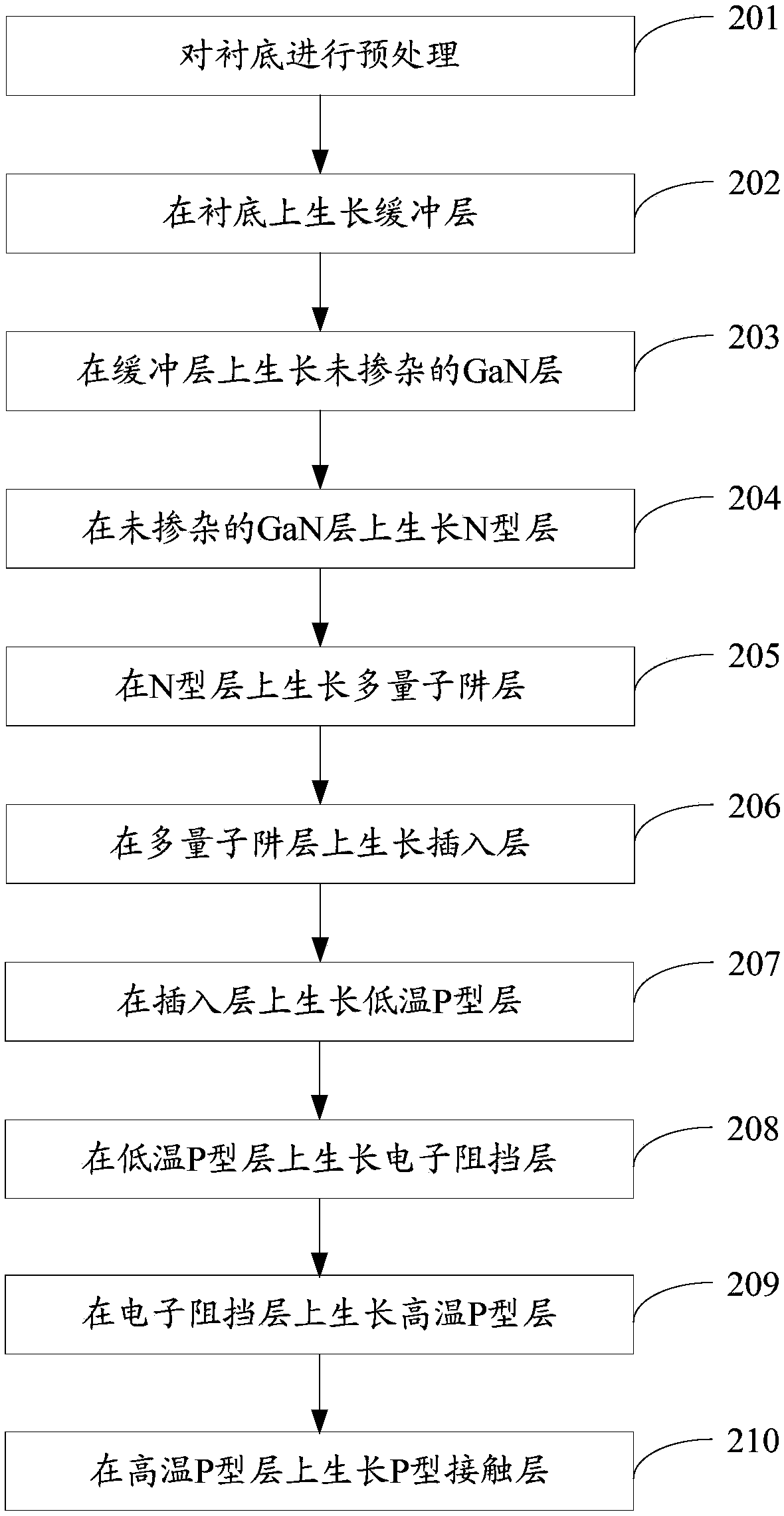
[0044] An embodiment of the present invention provides a method for manufacturing a light-emitting diode epitaxial wafer, which is suitable for the light-emitting diode epitaxial wafer provided in Embodiment 1. figure 2 It is a method flowchart of a method for manufacturing a light-emitting diode epitaxial wafer provided by an embodiment of the present invention, as shown in figure 2 As shown, the manufacturing method includes:
[0045] Step 201, performing pretreatment on the substrate.
[0046] Optionally, the substrate is sapphire with a thickness of 630-650um.
[0047] In this embodiment, Veeco K465i or C4MOCVD (Metal Organic Chemical VaporDeposition, metal organic compound chemical vapor deposition) equipment is used to realize the LED growth method. Using high-purity H 2 (hydrogen) or high-purity N 2 (nitrogen) or high purity H 2 and high purity N 2 The mixed gas as the carrier gas, high-purity NH 3 As the N source, trimethylgallium (TMGa) and triethylgallium (T...
Embodiment 3
[0079] An embodiment of the present invention provides a method for manufacturing a light-emitting diode epitaxial wafer. The manufacturing method provided in this embodiment is basically the same as that in Embodiment 2, except that in this embodiment, the low-temperature P-type layer It is an AlGaN / InGaN superlattice structure, the period number of the AlGaN / InGaN superlattice structure is 6, and the thickness is 21.6nm.
[0080] Specifically, when growing the AlGaN / InGaN superlattice structure of each period, it includes:
[0081] An AlGaN sublayer with a thickness of 1.8nm is grown for 30s, and an InGaN sublayer with a thickness of 1.8nm is grown for 30s.
[0082] The growth conditions of the AlGaN / InGaN superlattice structure are the same as the growth conditions of the AlGaN / GaN superlattice structure in Embodiment 2, and the present invention will not repeat them here.
[0083] After the growth of the light-emitting diode epitaxial wafer is finished, the temperature of...
PUM
| Property | Measurement | Unit |
|---|---|---|
| Doping concentration | aaaaa | aaaaa |
| Thickness | aaaaa | aaaaa |
| Thickness | aaaaa | aaaaa |
Abstract
Description
Claims
Application Information
 - R&D Engineer
- R&D Manager
- IP Professional
- Industry Leading Data Capabilities
- Powerful AI technology
- Patent DNA Extraction
Browse by: Latest US Patents, China's latest patents, Technical Efficacy Thesaurus, Application Domain, Technology Topic.
© 2024 PatSnap. All rights reserved.Legal|Privacy policy|Modern Slavery Act Transparency Statement|Sitemap