Wafer polishing method

一种晶圆、抛光头的技术,应用在磨削/抛光设备、电气元件、电路等方向,能够解决晶圆厚度不均匀、晶圆平坦度恶化、晶圆厚度均匀性恶化等问题,达到提高平坦度、抑制影响的效果

Active Publication Date: 2018-08-31
SUMCO CORP
View PDF10 Cites 11 Cited by
  • Summary
  • Abstract
  • Description
  • Claims
  • Application Information

AI Technical Summary

Problems solved by technology

[0012] However, in the conventional wafer polishing apparatus, even when a uniform polishing pressure is set in each pressure zone, there is a problem that a polishing pressure different from the set value is applied to a region where nano-topography exists. , thus deteriorating the uniformity of the wafer thickness
If the wafer is polished in this state, the polishing pressure will be concentrated on the convex part of the wafer surface, and since the polishing rate of the part with high polishing pressure is high, the thickness of the processed wafer will be reduced as shown in the figure. Inhomogeneity, the flatness of the wafer also deteriorates

Method used


Image

  • Wafer polishing method
  • Wafer polishing method
  • Wafer polishing method

Examples


Embodiment

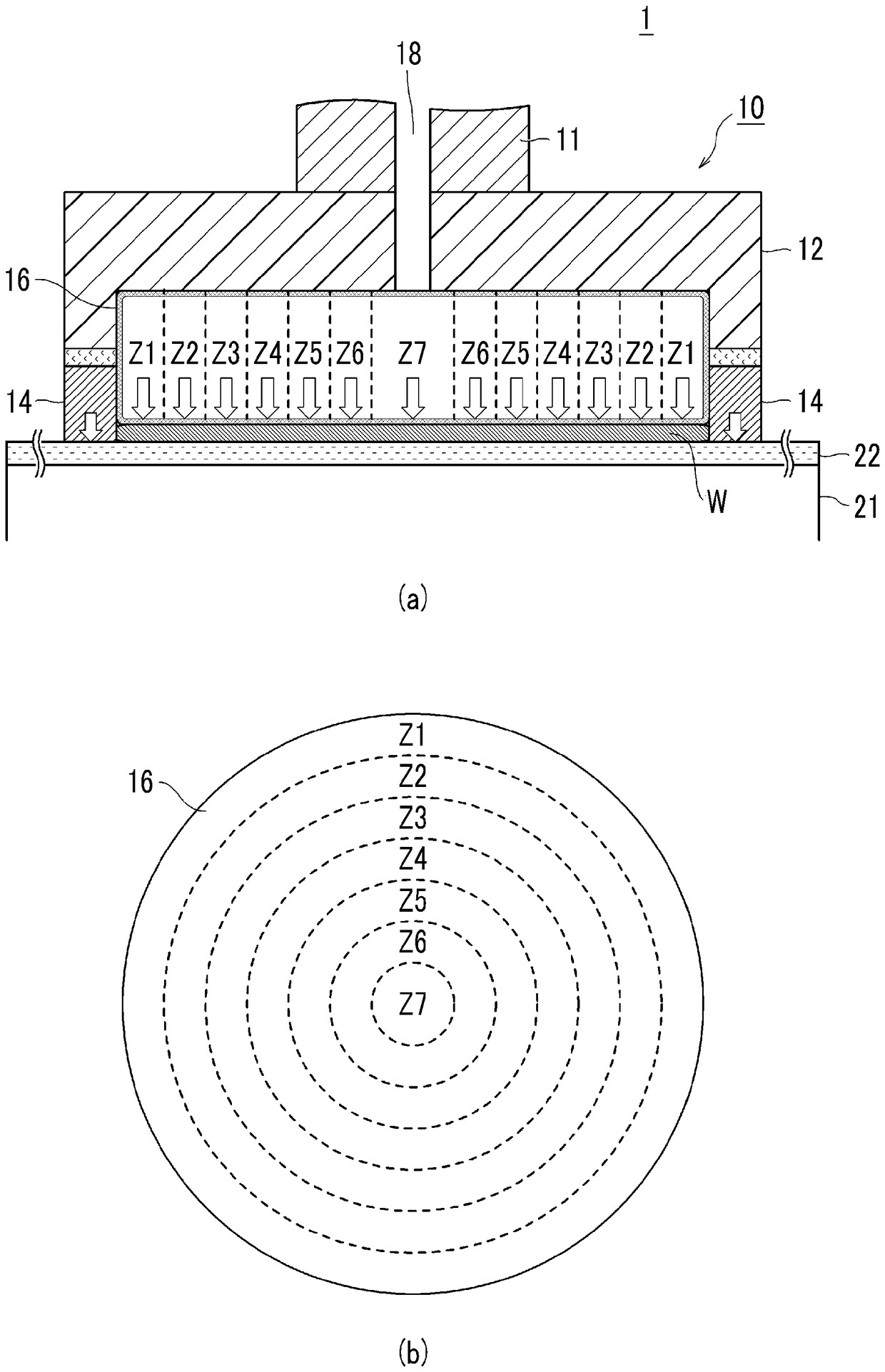
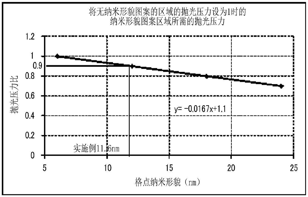
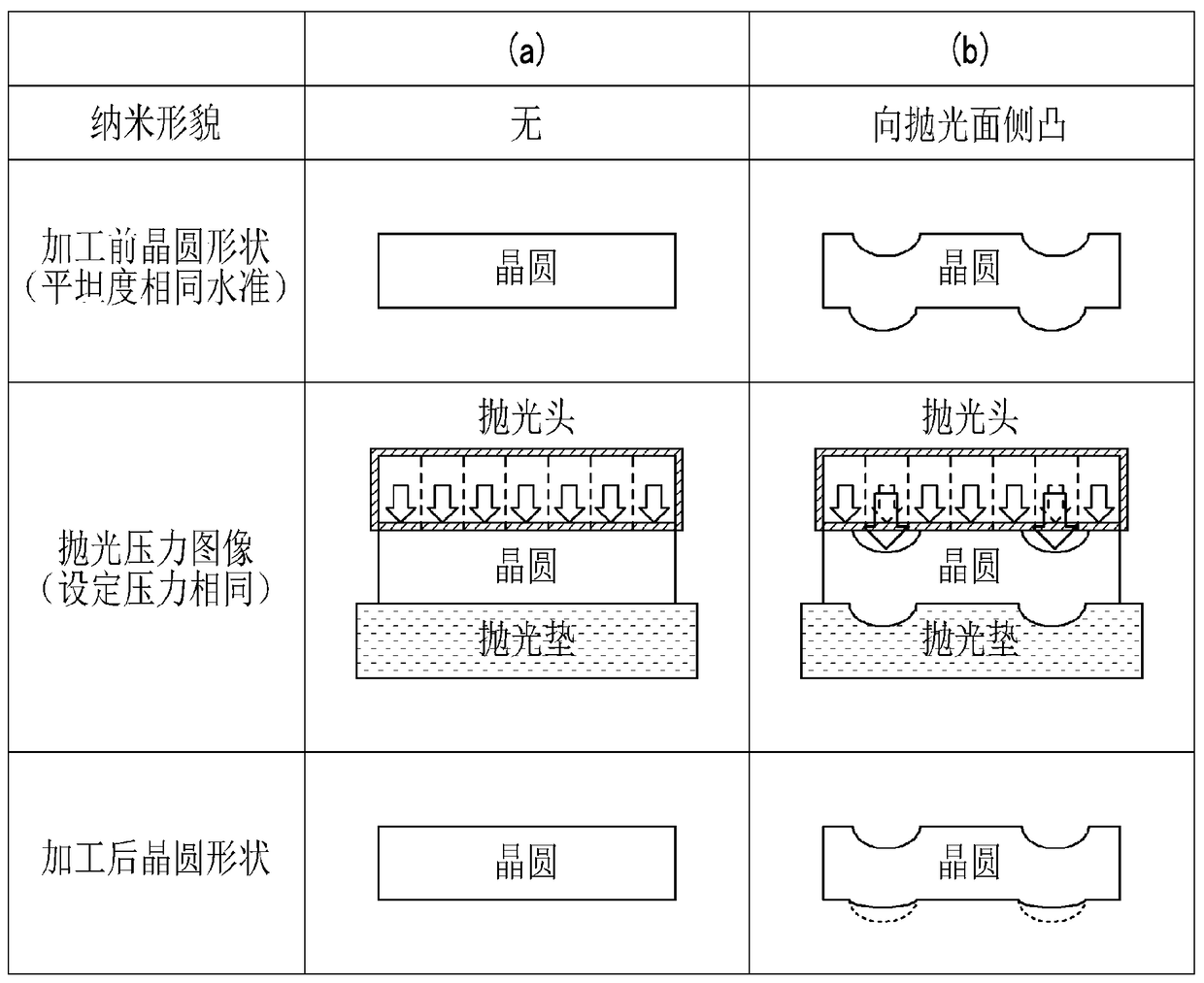
[0050] When performing mirror polishing on a wafer with nano-topography, evaluate the impact of the pressure control method of the polishing head on the flatness of the wafer. In the evaluation test, first, two samples of a 300-mm-diameter silicon single crystal wafer (wafer after double-side polishing) subjected to double-side grinding were prepared, and their nanotopography images were measured. The nanotopography was measured using an optical interferometric flatness / nanotopography measuring device (KLA Tecnor: "WaferSight3"). The grid point size in the wafer plane is 26mm×8mm, and the size of the nano-topography of each grid point is calculated and drawn as a graph.

[0051] Next, one and the other wafer samples were subjected to mirror polishing processing respectively by using the pressure control methods of the conventional and the present invention, to obtain polished wafers of comparative samples and example samples. That is, in the conventional pressure control meth...


PUM


Abstract

To apply, even if a wafer has nanotopography formed thereon, an appropriate polishing pressure to each pressure zone of the wafer while reducing influence from the nanotopography, and thereby, improvethe flatness of the wafer. This wafer polishing method is for mirror-polishing a surface of a wafer by using a wafer polishing device including a polishing head of a multiple zone pressurizing type capable of independently controlling pressurization of a plurality of pressure zones obtained by segmenting a pressured surface of the wafer. The wafer polishing method comprises: a measurement step for measuring a nanotopography map of the surface of the wafer (step S1); and polishing steps for setting, for each of the pressure zones, a polishing pressure from the polishing head to the wafer on the basis of the result of the measurement of the nanotopography map, and performing a polishing process (steps S2 and S3).

Description

technical field [0001] The invention relates to a method for polishing a wafer, in particular to a method for polishing a wafer with nano-morphology formed on the surface. Background technique [0002] Silicon wafers are widely used as substrate materials for semiconductor devices. A silicon wafer is manufactured by sequentially performing the following processes on a single crystal silicon ingot: peripheral grinding, slicing, lapping, etching, double-side polishing, single-side polishing, cleaning, and the like. Among them, the single-side polishing process is a necessary process for removing unevenness or undulations on the wafer surface to improve flatness, and the CMP (Chemical Mechanical Polishing: chemical mechanical polishing) method is used for mirror processing. [0003] Generally, a single-wafer wafer polishing apparatus (CMP apparatus) is used in a single-side polishing process of a silicon wafer. This wafer polishing device is equipped with a rotary table on wh...

Claims


Application Information

Patent Timeline
Patent Type & Authority Applications(China)
IPC IPC(8): H01L21/304
CPCB24B1/00H01L21/30625B24B37/005B24B37/30B24B49/12H01L21/0274H01L21/304B24B37/013H01L22/12
Inventor 西谷隆志谷本龙一
Owner SUMCO CORP
Why Eureka
Try Eureka