A surface modification method for suppressing the diffusion of conductive silver glue on the surface of the packaging substrate pad

A technology of conductive silver glue and packaging substrate, which is applied to the formation of conductive patterns, circuits, electrical components, etc., can solve problems such as abnormal wire bonding of conductive silver glue, and achieve the effect of realizing electrical connection and inhibiting diffusion.

Active Publication Date: 2020-12-29
UNIV OF ELECTRONICS SCI & TECH OF CHINA +1
View PDF6 Cites 0 Cited by
  • Summary
  • Abstract
  • Description
  • Claims
  • Application Information

AI Technical Summary

Problems solved by technology

[0004] The purpose of the present invention is to provide a surface modification method capable of suppressing the diffusion of conductive silver glue on the pad surface of the packaging substrate in view of the problem that the conductive silver glue diffuses on the surface of the pad in the prior art and seriously causes abnormal wire bonding, and then Facilitates connection between chip and external wiring lead frame

Method used


Image

  • A surface modification method for suppressing the diffusion of conductive silver glue on the surface of the packaging substrate pad
  • A surface modification method for suppressing the diffusion of conductive silver glue on the surface of the packaging substrate pad
  • A surface modification method for suppressing the diffusion of conductive silver glue on the surface of the packaging substrate pad

Examples


Embodiment 1

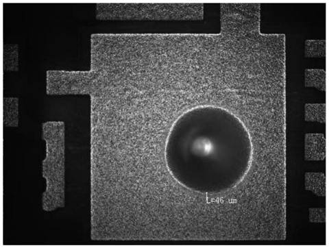
[0028] Step 1: Put the packaging substrate containing copper pads into the degreasing tank for degreasing treatment to remove oil stains such as oxides on the copper surface and finger marks. The degreasing time is 5 minutes, and the degreasing temperature is 50°C. After degreasing, use Ionized water cleaning; then put the substrate into the microetching solution system containing 5-aminotetrazole 3wt%, sulfuric acid 10wt%, hydrogen peroxide 8wt%, and carry out the planarity microetching of the copper pad, and the planarity microetching solution is carried out The temperature of the treatment is 25°C, the treatment time is 90s, and after the completion, it is cleaned with deionized water; at this time, a scanning electron microscope is used to observe the copper surface obtained after the pad is processed by the planar microetching system, and the results are as follows image 3 shown;

[0029] Step 2: Put the micro-etched substrate into the activation cylinder for ionic palla...

Embodiment 2

[0051] Step 1: Put the packaging substrate containing copper pads into the degreasing tank for degreasing treatment to remove oil stains such as oxides on the copper surface and finger marks. The degreasing time is 5 minutes, and the degreasing temperature is 50°C. After degreasing, use Ionized water cleaning; then put the substrate into the microetching solution system containing 2-methyl-5-aminotetrazole 2wt%, sulfuric acid 18wt%, hydrogen peroxide 10wt%, and carry out the planarity microetching of the copper pad, smooth The temperature of the microetching solution is 25°C, the treatment time is 90s, and it is cleaned with deionized water after completion;

[0052] Step 2: Put the microetched substrate into the activation cylinder for ionic palladium activation treatment, the activation time is 100s, the activation temperature is 30°C, and after activation, it is cleaned with deionized water; the activated substrate is placed in the nickel cylinder, Electroless nickel, palla...

Embodiment 3

[0057] Step 1: Put the packaging substrate containing copper pads into the degreasing tank for degreasing treatment to remove oil stains such as oxides on the copper surface and finger marks. The degreasing time is 5 minutes, and the degreasing temperature is 50°C. After degreasing, use Ionized water cleaning; then put the substrate into the microetching solution system containing 5-aminotetrazole 2wt%, 2-methyl-5-aminotetrazole 2wt%, sulfuric acid 6wt%, hydrogen peroxide 12wt%, and carry out copper The flatness micro-etching of the pad, the temperature of the flatness micro-etching solution is 25°C, the processing time is 90s, and it is cleaned with deionized water after completion;

[0058] Step 2: Put the micro-etched substrate into the activation cylinder for ionic palladium activation treatment, the activation time is 200s, the activation temperature is 15°C, and after activation, clean it with deionized water; put the activated substrate into the nickel cylinder, Electro...


PUM


Abstract

The invention discloses a surface modification method for suppressing the diffusion of conductive silver glue on the surface of a pad on a packaging substrate, belonging to the technical field of surface treatment of packaging substrates. In the present invention, nickel-palladium-gold modification is performed on the surface of the copper pad before the conductive silver glue is applied: first, the surface of the copper pad is etched with a flat micro-etching solution, and then electroless nickel, palladium and gold are sequentially plated after activation. The gold layer is then heat-treated in a vacuum inert environment. On the one hand, the present invention adds a corrosion inhibitor to the traditional sulfuric acid / hydrogen peroxide micro-etching system to avoid the formation of a relatively rough copper surface during the micro-etching process; Therefore, the serious diffusion of the conductive silver glue on the surface of the pad is effectively suppressed, and the diffusion range of the conductive silver glue to the surroundings can be controlled within 50 μm, which is beneficial to realize the effective electrical connection of the components in the circuit. Therefore, the present invention is applicable to the modification of copper pads of printed circuit boards and packaging substrates.

Description

technical field [0001] The invention relates to the technical field of surface treatment of packaging substrates, in particular to a surface modification method for suppressing the diffusion of conductive silver glue on the pad surface of the packaging substrate. Background technique [0002] The packaging of electronic products refers to connecting the circuit pins on the internal chip to the external joints with wires so as to connect with other devices. The package not only plays the role of installation, fixing, sealing, protecting the chip and enhancing the electrothermal performance, but also fixes the chip on the substrate through the lead hole on the substrate, and uses wires to connect the pad to the pin of the package shell. These pins are connected to other devices through wires on the printed circuit board, so as to realize the connection between the internal chip and the external circuit. At present, conductive silver glue is usually used as the packaging adhes...

Claims


Application Information

Patent Timeline
Patent Type & Authority Patents(China)
IPC IPC(8): H01L21/48C23F1/18C23C18/42C23C18/32C23C18/18H05K3/10
CPCC23C18/1831C23C18/32C23C18/42C23F1/18H01L21/4828H05K3/10
Inventor 陈苑明贾莉萍何为夏锋晋晓峰陈庆国王守绪
Owner UNIV OF ELECTRONICS SCI & TECH OF CHINA
Why Eureka
Try Eureka