Square flat chip packaging structure with high electromagnetic pulse interference resistance

A chip packaging structure, electromagnetic pulse technology, applied in the direction of circuits, electrical components, electrical solid devices, etc., can solve problems such as permanent failure of electronic devices, damage to electronic systems, and instrument crashes, so as to improve the ability to resist electromagnetic pulse interference and facilitate Batch processing, good effect of implementation

Active Publication Date: 2020-09-11
XIAN UNIV OF SCI & TECH
View PDF11 Cites 0 Cited by
  • Summary
  • Abstract
  • Description
  • Claims
  • Application Information

AI Technical Summary

Problems solved by technology

However, the inevitable co-working of a large number of electronic devices has led to the emergence of electromagnetic compatibility problems, especially for semiconductor devices with increasing integration, microwave interference and flipping effects have become increasingly serious
All kinds of electromagnetic interference from the outside can be input into the electronic system through various coupling channels, causing problems such as computer errors, equipment restarts, and instrument crashes. In serious cases, some electronic devices will permanently fail. damage, which brings great inconvenience to people's lives
As a new electromagnetic interference source that has attracted widespread attention, high-power microwaves cause interference and damage to electronic and electrical systems and facilities, which may lead to circuit failure and system paralysis.

Method used


Image

  • Square flat chip packaging structure with high electromagnetic pulse interference resistance
  • Square flat chip packaging structure with high electromagnetic pulse interference resistance
  • Square flat chip packaging structure with high electromagnetic pulse interference resistance

Examples


Embodiment Construction

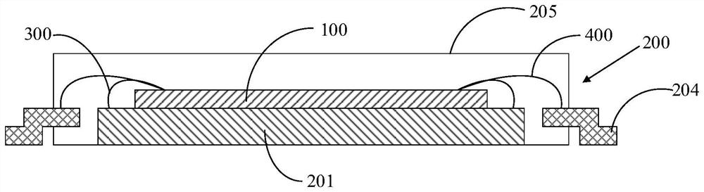
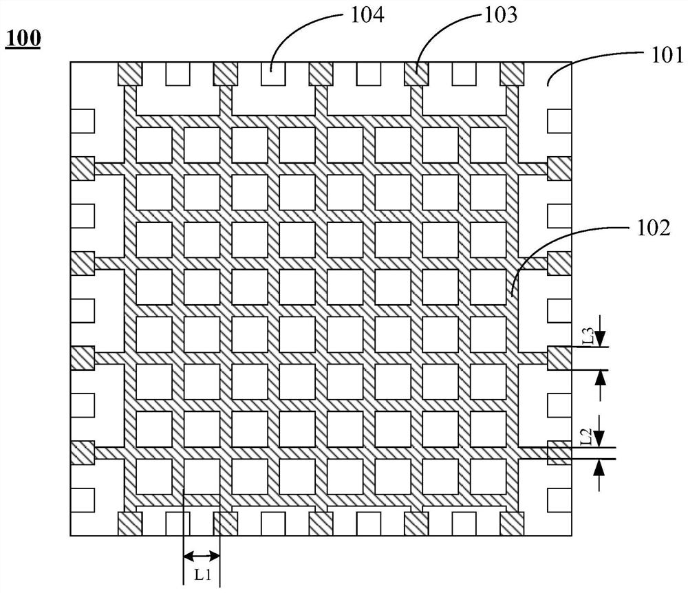
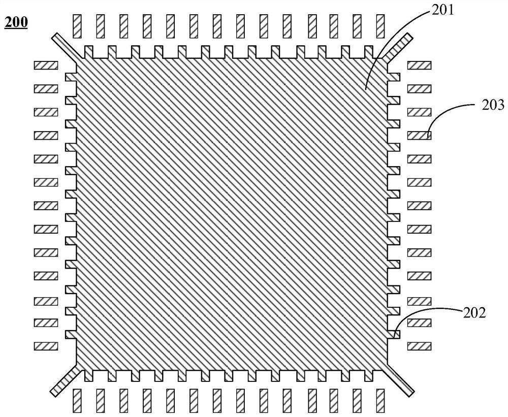
[0030] In order to further explain the technical means and effects of the present invention to achieve the intended purpose of the invention, a quadrilateral flat chip packaging structure with high electromagnetic pulse interference resistance proposed according to the present invention will be described in detail below in conjunction with the accompanying drawings and specific implementation methods. illustrate.

[0031] The aforementioned and other technical contents, features and effects of the present invention can be clearly presented in the following detailed description of specific implementations with accompanying drawings. Through the description of specific embodiments, the technical means and effects of the present invention to achieve the intended purpose can be understood more deeply and specifically, but the accompanying drawings are only for reference and description, and are not used to explain the technical aspects of the present invention. program is limited....


PUM


Abstract

The invention relates to a square flat chip packaging structure with high electromagnetic pulse interference resistance. The square flat chip packaging structure comprises a bare chip and a packagingpiece. The bare chip comprises a bare chip main body, a shielding structure and a plurality of first pins are arranged on the bare chip main body, and the plurality of first pins are connected with the shielding structure. The packaging piece comprises a lead frame main body and a first bonding pad, the bare chip main body is arranged on the lead frame main body, and the first bonding pad is connected with the lead frame main body; the first pins are connected with the first bonding pad through first bonding wires. According to the square flat chip packaging structure, the shielding structureis formed on the upper surface of the bare chip body, the first pins connected with the shielding structure are in bonding connection with the first bonding pad through the bonding wires, the shielding shell wrapping the bare chip body is formed, and electromagnetic pulse interference resistance can be achieved without developing a special shielding shell.

Description

technical field [0001] The invention belongs to the technical field of electromagnetic pulse protection, and in particular relates to a square flat chip package structure with high anti-electromagnetic pulse interference capability. Background technique [0002] Package refers to the shell used to install the semiconductor integrated circuit chip. It not only plays the role of placing, fixing, sealing, protecting the chip and enhancing thermal conductivity, but also serves as a bridge to communicate the internal world of the chip with the external circuit - the contact wire on the chip Connect to pins on the package case, which in turn connect to other devices via wires on the printed circuit board. QFP (Quad Flat Package) is a new packaging form specially developed for small pin pitch surface mount IC chips (Integrated Circuit Chip). QFP is a packaging form that adapts to the increase of IC chip capacity and the increase in the number of I / Os, and has been widely used at p...

Claims


Application Information

Patent Timeline
IPC IPC(8): H01L23/552H01L23/495
CPCH01L23/552H01L23/49541H01L2224/48257H01L2224/48247H01L2224/48091H01L2924/181H01L2924/00014H01L2924/00012
Inventor 李妤晨
Owner XIAN UNIV OF SCI & TECH
Why Eureka
Try Eureka