Lighting device manufacturing method

A manufacturing method and lighting device technology, applied in the direction of electrical components, electrical solid devices, circuits, etc., can solve problems such as difficulty in finding LED chips, inability to adjust and change series and parallel connections, and achieve flexible wiring, reduced use, and good conductivity Effect

Active Publication Date: 2018-09-04
临沂兴创达知识产权运营有限公司
View PDF5 Cites 3 Cited by
  • Summary
  • Abstract
  • Description
  • Claims
  • Application Information

AI Technical Summary

Problems solved by technology

For example attached figure 1 A plurality of LED chips 2 are mounted on an insulating substrate 1, and the LED chips 2 are flip-chip mounted on a circuit pattern (not shown) on the insulating substrate 1 via solder balls 3, and finally sealed via an encapsulating resin 4. The surface of this package The light source needs to form a circuit pattern on the insulating substrate 1 in advance. After the circuit pattern is encapsulated, the series and parallel connection cannot be adjusted and changed. In addition, after a certain LED chip fails, it is difficult to find the failed LED chip.

Method used


Image

  • Lighting device manufacturing method
  • Lighting device manufacturing method
  • Lighting device manufacturing method

Examples


Embodiment Construction

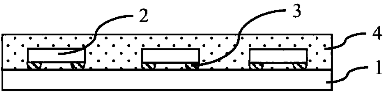
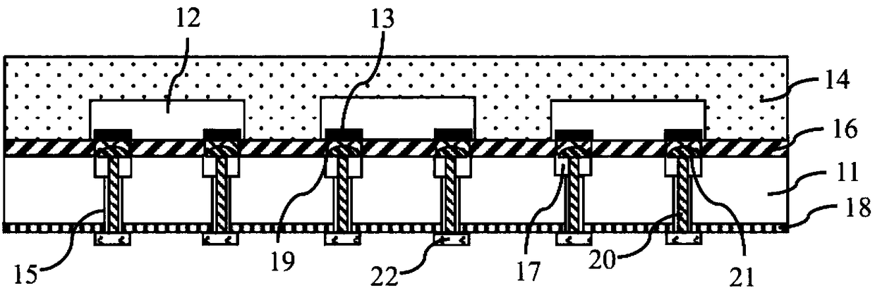
[0024] see figure 2 , the lighting device of the present invention, which comprises:

[0025] An insulating substrate 11, the insulating substrate 11 has opposite first surface and second surface, a plurality of notches 17 are arranged on the first surface, and the interior of the insulating substrate 11 also includes A plurality of through holes 15 on the bottom surface and the second surface, and its thickness is d1;

[0026] The adhesive layer 16, whose thickness is d2, is arranged on the first surface, and has a plurality of grooves 19 corresponding to the plurality of notches 17, and the plurality of grooves 19 are connected to the plurality of notches 17. The notches 17 are connected to each other;

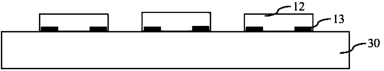
[0027] A plurality of LED chips 12, adhered to the adhesive layer 16, and have a plurality of electrode pads 13, the plurality of electrode pads 13 respectively correspond to the plurality of grooves 19 and in the plurality of grooves exposed in the groove 19;

[0028] ...


PUM


Abstract

The invention provides a lighting device manufacturing method. A circuit pattern on the lower surface of an insulation substrate is led out through notches, grooves and through holes. The circuit pattern can realize flexible wiring, and helps search of a failed LED chip, and detection of the plurality of through holes can be realized; conductive nails can prevent overflow of conductive paste, andreduce use of the conductive paste, and conductivity is better; and through a lift plate, electrical connection between the conductive paste and electrode welding plates is realized easily and reliably.

Description

technical field [0001] The invention relates to the field of LED package manufacturing, in particular to a method for manufacturing an illuminating device. Background technique [0002] Most of the existing LED packages are in the form of COB, which utilizes circuit patterns on an insulating substrate to realize series-parallel connection of LEDs. For example attached figure 1 A plurality of LED chips 2 are mounted on an insulating substrate 1, and the LED chips 2 are flip-chip mounted on a circuit pattern (not shown) on the insulating substrate 1 via solder balls 3, and finally sealed via an encapsulating resin 4. The surface of this package The light source needs to form a circuit pattern on the insulating substrate 1 in advance. After the circuit pattern is encapsulated, the series and parallel connection cannot be adjusted and changed. In addition, after a certain LED chip fails, it is difficult to find the failed LED chip. Contents of the invention [0003] Based on...

Claims


Application Information

Patent Timeline
Patent Type & Authority Applications(China)
IPC IPC(8): H01L25/075H01L33/48H01L33/62H01L33/00
CPCH01L25/0753H01L33/005H01L33/48H01L33/62
Inventor 孙爱芬
Owner 临沂兴创达知识产权运营有限公司
Why Eureka
Try Eureka