
Pixel structure, mask and display device

A technology of pixel structure and mask plate, which is applied in the direction of vacuum evaporation plating, coating, electric solid device, etc., can solve the problems of FMM process implementation difficulty and cannot meet the high PPI development requirements of OLED display devices, and achieve the reduction of manufacturing process And the difficulty of the evaporation process, the effect of good display effect and uniform color distribution

Active Publication Date: 2019-07-23
KUNSHAN GO VISIONOX OPTO ELECTRONICS CO LTD
View PDF11 Cites 0 Cited by
  • Summary
  • Abstract
  • Description
  • Claims
  • Application Information

AI Technical Summary

Problems solved by technology

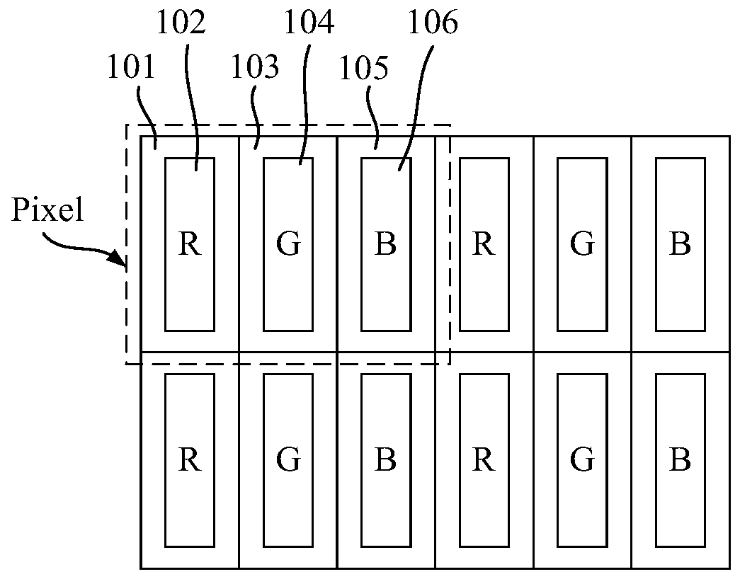
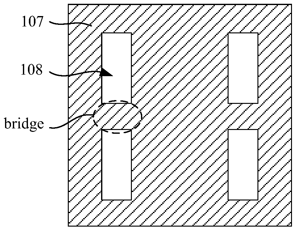
FMM generally has a minimum opening limit, and the sub-pixels of different colors in the evaporation process are limited by the opening pitch. The fabrication of OLED pixel structures will inevitably be limited by the FMM opening and the precision of the evaporation process. Figure 1A As shown in the pixel structure, when the pixel density is higher than 300PPI (Pixel Per Inch, pixel density), the current FMM process is very difficult to implement, and cannot meet the high PPI development requirements of OLED display devices.

Method used


Image

  • Pixel structure, mask and display device
  • Pixel structure, mask and display device
  • Pixel structure, mask and display device

Examples


Embodiment Construction

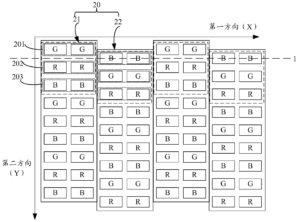
[0026] After research, the applicant found that the traditional RGB pixel structure can no longer meet the requirements of high PPI display effect of the product. Based on this, the present invention provides a pixel structure, including a plurality of pixel groups arranged in an array, each of the pixel groups includes a first pixel group and a second pixel group that are adjacently arranged and mutually misaligned, and the first pixel group Both the second pixel group and the second pixel group include sub-pixel groups with three different colors, and the arrangement orders of the three different-color sub-pixel groups in the first pixel group and the second pixel group are different; each sub-pixel group includes At least two sub-pixels of the same color are respectively adjacently arranged. In this pixel structure, the first pixel group and the second pixel group of the pixel group are adjacent and dislocated, and the two sub-pixels of the same color in each pixel group ca...


PUM


Abstract

The present invention provides a pixel structure, a mask plate and a display device. The pixel structure includes a plurality of large groups of pixels arranged in an array, and each large group of pixels includes first pixel subgroups and The second pixel group, the first pixel group and the second pixel group respectively include three sub-pixel groups with different colors, and the three sub-pixel groups with different colors are in the first pixel group and the second pixel group The order of arrangement is not the same, each sub-pixel group contains at least two sub-pixels of the same color, and at least two sub-pixels of the same color can share one evaporation opening, thus ensuring that the sub-pixel groups of the same color are regularly interlaced arrangement, thereby increasing the strength of the mask plate, which is beneficial to manufacturing small-sized sub-pixels and improving the PPI of the display device.

Description

technical field [0001] The invention relates to the field of display technology, in particular to a pixel structure, a mask plate and a display device. Background technique [0002] OLED (Organic Light-Emitting Diode, Organic Light-Emitting Diode) display technology has the characteristics of self-illumination, because of its large viewing angle of the display screen and the advantages of saving power, it has been widely used in mobile phones, digital cameras, DVD players, personal In products such as digital assistants (PDAs), notebook computers, car stereos, and televisions. [0003] At present, the pixel structure of a typical OLED display panel is arranged in a side-by-side way. In this side-by-side way, there are red, green, There are three blue (R, G, B) sub-pixels, each sub-pixel is rectangular, and each has an independent organic light-emitting device. Specifically, such as Figure 1A As shown, each pixel unit Pixel includes R (red) sub-pixels 101, G (green) sub-pi...

Claims


Application Information

Patent Timeline
Patent Type & Authority Patents(China)
IPC IPC(8): H01L27/32H01L51/56C23C14/04
CPCC23C14/042H10K59/353H10K71/166
Inventor 侯炜轩李俊峰刘明星王徐亮高峰
Owner KUNSHAN GO VISIONOX OPTO ELECTRONICS CO LTD
Learn More