PCB board riveting anti-offset jig

A technology for riveting and sheet materials, which is applied in the manufacture of multilayer circuits, electrical components, and printed circuits. combined effect

Pending Publication Date: 2018-09-07
JIANGSU BOMIN ELECTRONICS
View PDF0 Cites 0 Cited by
  • Summary
  • Abstract
  • Description
  • Claims
  • Application Information

AI Technical Summary

Problems solved by technology

[0003] The existing riveting process has the following defects: Since the stacked layers of the PCB boards to be riveted are not pre-fixed, before the formal riveting, it is very easy to generate interlayer slippage during the transfer process of the laminated layers Offset, thus affecting the riveting effect

Method used


Image

  • PCB board riveting anti-offset jig
  • PCB board riveting anti-offset jig
  • PCB board riveting anti-offset jig

Examples


Embodiment Construction

[0018] In order to illustrate the idea and purpose of the present invention, the present invention will be further described below in conjunction with specific embodiments.

[0019] First of all, "one embodiment" or "embodiment" referred to herein refers to a specific feature, structure or characteristic that may be included in at least one implementation of the present invention. "In one embodiment" appearing in different places in this specification does not all refer to the same embodiment, nor is it a separate or selective embodiment that is mutually exclusive with other embodiments.

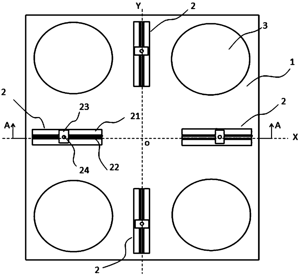
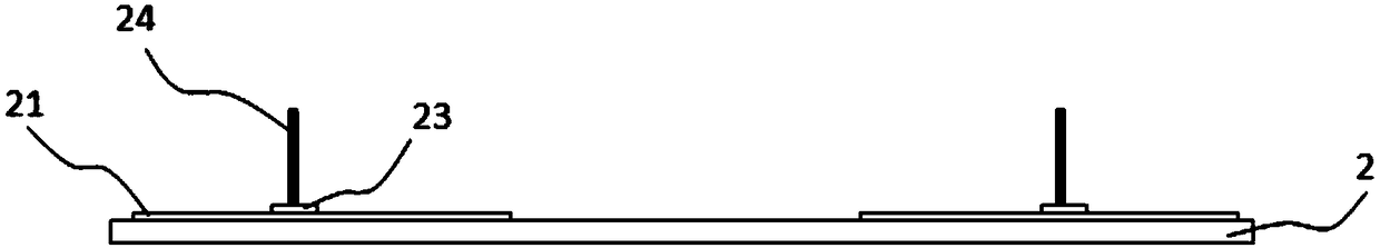
[0020] Such as figure 1 , figure 2 As shown, in a specific embodiment, the riveting anti-deflection jig provided by the present invention includes a rectangular base plate 1 and four sliding positioning components 2 arranged on the base plate 1 .

[0021] In this embodiment, the length of the long side a of the substrate 1 is 28 inches, the length of the short side b of the substrate 1 i...


PUM


Abstract

The invention discloses a PCB board riveting anti-offset jig, which comprises a rectangular substrate, and four sliding positioning components disposed on the substrate, wherein two of the sliding positioning components are disposed on a long-edge middle line of the substrate and symmetrically distributed on the two sides of the short-edge middle line of the substrate, and the other two sliding positioning components are disposed on the short-edge middle line of the substrate and symmetrically distributed on the two sides of the long-edge middle line of the substrate; each of the sliding positioning components comprises a linear guide rail and a sliding block, which is connected to the linear guide rail and slidable along the linear guide rail; a positioning rod is connected to the slidingblock and perpendicular to the substrate; and the cross-sectional diameter of the positioning rod matches the aperture of the positioning hole on a PCB board to be riveted. The PCB board riveting anti-offset jig in the invention can satisfy riveting pre-positioning of PCB boards of various sizes, thereby preventing the superposed layer of the PCB board from inter-layer sliding offset before riveting, and finally ensuring the riveting effect.

Description

technical field [0001] The invention belongs to the field of printed circuit board manufacturing, and more specifically relates to a riveting anti-deviation jig for PCB boards. Background technique [0002] Riveting is a common process that must be implemented in the production process of PCB boards. The traditional method is to stack the PCB boards to be riveted (including PCB substrates and PP boards), and then use a riveting machine to rivet them. Such as image 3 As shown, in order to realize the riveting of the PCB boards 100 to be riveted, a positioning hole 101 is generally drilled at the center of the four edges of each PCB board 100, and then the PCB boards 100 are stacked sequentially according to the requirements. Finally, the laminated layer is assembled to a riveting machine through the positioning hole 101 for riveting. [0003] The existing riveting process has the following defects: Since the stacked layers of the PCB boards to be riveted are not pre-fixed, ...

Claims


Application Information

Patent Timeline
Patent Type & Authority Applications(China)
IPC IPC(8): H05K3/46
CPCH05K3/4638
Inventor 徐缓王庆军傅廷昌
Owner JIANGSU BOMIN ELECTRONICS
Why Eureka
Try Eureka