Test method and system for testing internal eye diagram of chip

A technology of internal signals and test methods, applied in the direction of electronic circuit testing, measuring electricity, measuring devices, etc., can solve problems such as errors and inaccurate test results, and achieve the effect of low cost of use, convenient parameter adjustment, and guaranteed consistency.

Inactive Publication Date: 2018-09-14
ZHENGZHOU YUNHAI INFORMATION TECH CO LTD
View PDF7 Cites 14 Cited by
  • Summary
  • Abstract
  • Description
  • Claims
  • Application Information

AI Technical Summary

Problems solved by technology

[0005] The present invention proposes a test method and system for testing the internal signal eye diagram of a chip, which is used to solve the problem that there is an error between the results obtained by the existing chip test method and the test results and the actual signal inside the chip, resulting in inaccurate test results

Method used


Image

  • Test method and system for testing internal eye diagram of chip
  • Test method and system for testing internal eye diagram of chip
  • Test method and system for testing internal eye diagram of chip

Examples


Embodiment Construction

[0024] In order to make the purpose, technical solutions and advantages of the embodiments of the present invention clearer, the technical solutions in the embodiments of the present invention will be clearly and completely described below in conjunction with the drawings in the embodiments of the present invention. Obviously, the described embodiments It is a part of embodiments of the present invention, but not all embodiments.

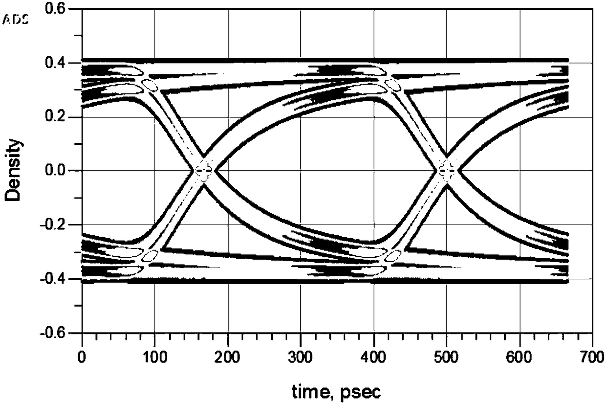
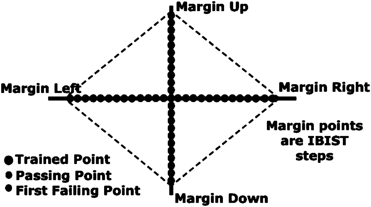
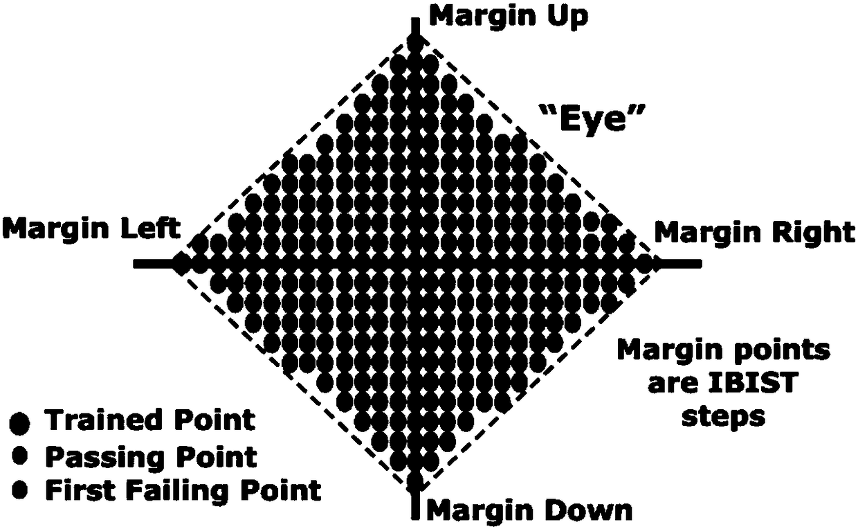
[0025] Such as Figure 1-Figure 3 As shown, this embodiment discloses a test method for testing the internal signal eye diagram of the chip, including the following steps:

[0026] S1. Lap the test platform, and input a reference voltage signal and a clock signal at the receiving end of the chip to be tested to obtain sampling points;

[0027] S2. Adjust the phase of the clock signal and the size of the reference voltage signal to change the position of the sampling point, and test the acquired sampling point to obtain a boundary sampling point whe...


PUM


Abstract

The invention discloses a test method and system for testing an internal eye diagram of a chip. The method comprises the following steps: S1, erecting a test platform and inputting a reference voltagesignal and a clock signal at a to-be-tested chip receiving end to obtain a sampling point; S2, adjusting a clock signal phase and a reference voltage signal to change the location of the sampling point, and testing the obtained sampling point to obtain a boundary sampling point with an error code; S3, repeated the previous step to obtain a plurality of boundary sampling points, connecting the boundary sampling points to form a boundary contour of an internal signal of the chip so as to obtain eye height and eye width data and a signal simulation eye diagram; and S4, compensating the referencevoltage signal and the clock signal and determining the compensated eye height and eye width data to obtain a final internal signal eye diagram of the chip. According to the invention, with internalsimulation testing, parameter adjustment becomes convenient; the consistency of the testing result and the internal actual signal of the chip is ensured; and the precision of the chip signal eye diagram result is improved.

Description

technical field [0001] The invention relates to the field of chip testing, in particular to a testing method and system for testing an internal signal eye diagram of a chip. Background technique [0002] For chip testing for high-speed signal processing, there is usually De-emphasis at the sending end, and DFE and CTLE at the receiving end. The two work together to ensure that the eye diagram of the signal at the receiving end meets the requirements. The traditional high-speed signal test method is to connect the fixture test at the receiving end, or solder or spot test at the receiving end, and then use an oscilloscope to analyze the eye diagram. [0003] The above test method has two disadvantages: First, the signal is tested outside the chip at the receiving end, and it is necessary to simulate the effect of DFE and CTLE on the signal at the receiving end of the chip to obtain the final eye diagram. Generally, the DFE and CTLE are simulated inside the oscilloscope. CTLE ...

Claims


Application Information

Patent Timeline
Patent Type & Authority Applications(China)
IPC IPC(8): G01R31/28
CPCG01R31/2894
Inventor 许晓平
Owner ZHENGZHOU YUNHAI INFORMATION TECH CO LTD
Why Eureka
Try Eureka