Silicon carbide junction barrier Schottky diode

A technology of junction barrier Schottky and diodes, which is applied in the direction of electrical components, circuits, semiconductor devices, etc., can solve the problem of low utilization rate of structural design area, achieve large area factor, large forward current density, and area utilization rate high effect

Pending Publication Date: 2018-09-14
SHENZHEN BASIC SEMICON LTD
View PDF0 Cites 0 Cited by
  • Summary
  • Abstract
  • Description
  • Claims
  • Application Information

AI Technical Summary

Problems solved by technology

[0004] The main purpose of the present invention is to propose a silicon carbide junction barrier Schottky diode with an improved area factor by improving the struc

Method used


Image

  • Silicon carbide junction barrier Schottky diode
  • Silicon carbide junction barrier Schottky diode
  • Silicon carbide junction barrier Schottky diode

Examples


Example Embodiment

[0018] The present invention will be further described below in conjunction with the accompanying drawings and specific embodiments.

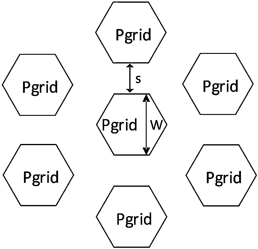
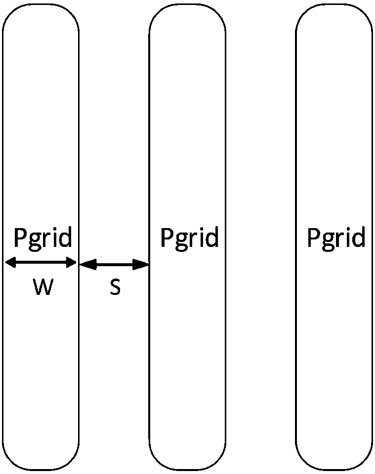
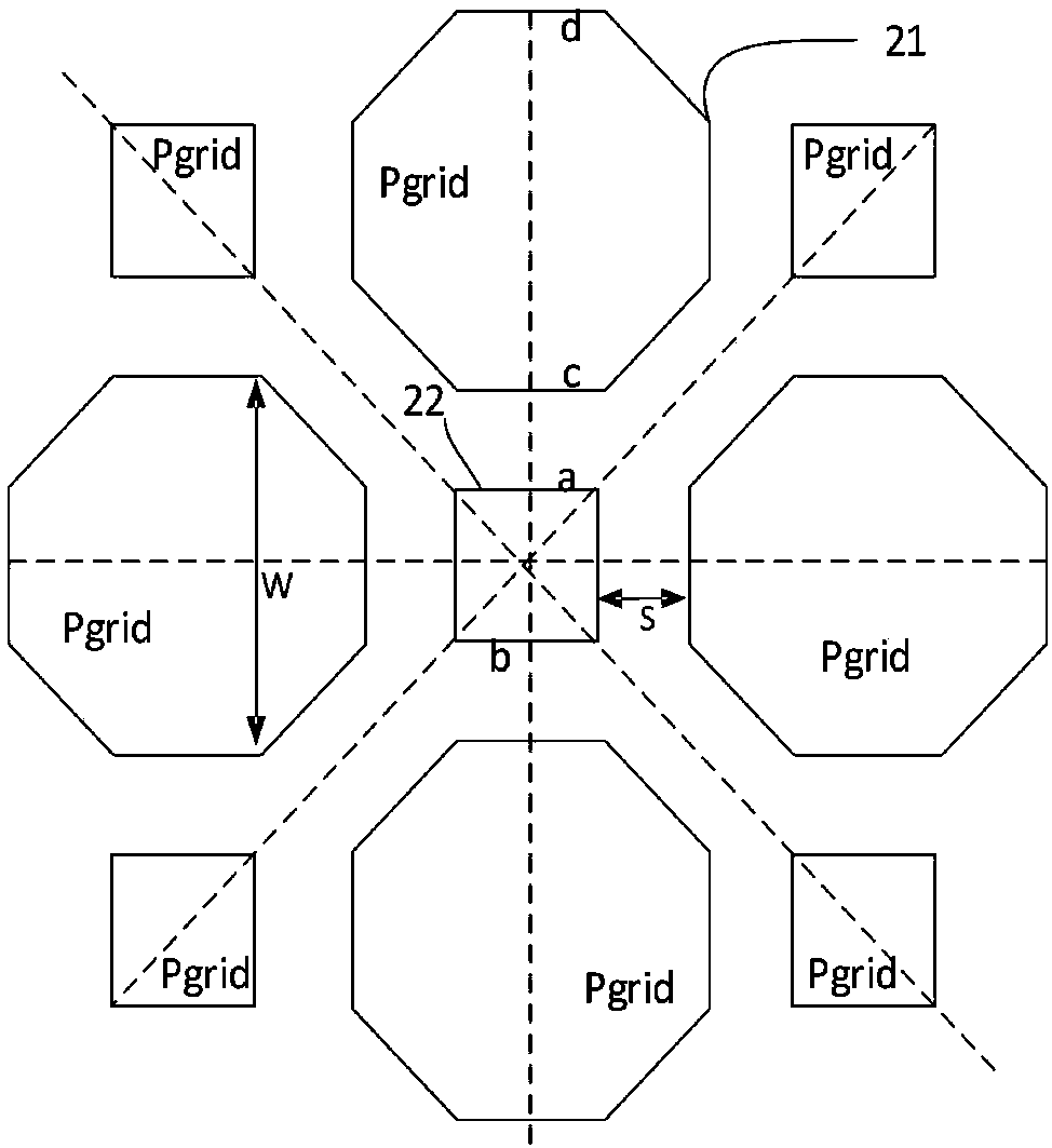
[0019] A silicon carbide junction barrier Schottky diode (or "SIC JBS device") has a cell chip area and a terminal terminal area. Among them, the P-type ion-implanted doped region (referred to as "Pgrid") in the chip area is a region that prevents the passage of current. When the device is turned off in reverse, Pgrid will widen the PN junction due to the reverse voltage applied to the PN junction. The width of the depletion region is used to shut off the current and realize the reverse current cut-off characteristics of the device; the other areas of the chip area are current conduction areas. The area factor is one of the parameters that characterize the performance of the device. When other parameters are the same, the larger the area factor, the higher the area utilization rate and the greater the forward current density. Area factor=(tota...


PUM


Abstract

The present invention discloses a silicon carbide junction barrier Schottky diode (SIC JBS). The diode comprises octagonal and square P-type ion implantation doping areas (2), and the octagonal P-typeion implantation doping area (21) and the square P-type ion implantation doping area (22) are alternately arranged at equal intervals. According to the silicon carbide junction barrier Schottky diodedevice, the P-type ion implantation doping areas are designed to an octagonal shape and a square shape, and the octagonal P-type ion implantation doping area (21) and the square P-type ion implantation doping area (22) are alternately arranged at equal intervals to allow the area utilization of the device chip area to be higher and obtain larger area factors so as to allow the forward current density of the device to be higher.

Description

technical field [0001] The invention relates to a semiconductor device, in particular to a silicon carbide junction barrier Schottky diode which improves the design of a P-type ion implantation doping region. Background technique [0002] In SIC JBS (Silicon Carbide Junction Barrier Schottky Diode) devices, Pgrid (P-type ion implanted doped region) is a region that prevents the passage of current. In the current mainstream devices of SIC JBS, the structure of Pgrid is mostly designed as figure 1 The regular hexagon shown and as figure 2 As shown in the strip shape, however, these two mainstream designs are still lacking in area utilization, and the area factor needs to be improved. [0003] The disclosure of the above background technical content is only used to assist in understanding the inventive concepts and technical solutions of the present invention, and it does not necessarily belong to the prior art of this patent application. There is no clear evidence that the a...

Claims


Application Information

Patent Timeline
IPC IPC(8): H01L29/872H01L29/06
CPCH01L29/872H01L29/0615
Inventor 张振中林盛杰和巍巍汪之涵
Owner SHENZHEN BASIC SEMICON LTD
Why Eureka
Try Eureka