Liquid crystal display device

A technology of liquid crystal display devices and liquid crystal display panels, applied in static indicators, instruments, optics, etc., can solve the problems of large frame width, small screen-to-body ratio, difficulty in meeting the narrow frame design requirements of liquid crystal display devices, etc., and achieve reduction The effect of border width and increasing screen ratio

Active Publication Date: 2018-10-02
SHANGHAI AVIC OPTOELECTRONICS
View PDF34 Cites 11 Cited by
  • Summary
  • Abstract
  • Description
  • Claims
  • Application Information

AI Technical Summary

Problems solved by technology

Wherein, the driving array is arranged in the display area, the control chip and the fan-out wiring electrically connected with the control chip are arranged in the frame area of ​​the liquid crystal display device; at the same time, the light source in the backlight module is also located in the frame area of ​​the liquid crystal display device, and the light source is connected to the frame area of ​​the liquid crystal display device. There also needs to be a certain distance between the light incident surfaces of the light guide plate to increase the light mixing effect. Therefore, the existing liquid crystal display device has a large frame width and a small screen-to-body ratio, which is difficult to meet the design requirements of the narrow frame of the liquid crystal display device.

Method used


Image

  • Liquid crystal display device
  • Liquid crystal display device
  • Liquid crystal display device

Examples


Embodiment Construction

[0027] The present invention will be further described in detail below in conjunction with the accompanying drawings and embodiments. It should be understood that the specific embodiments described here are only used to explain the present invention, but not to limit the present invention. In addition, it should be noted that, for the convenience of description, only some structures related to the present invention are shown in the drawings but not all structures.

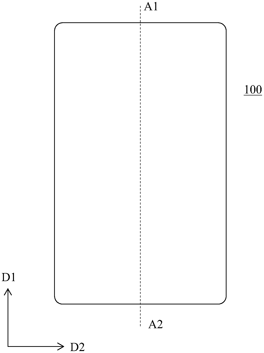
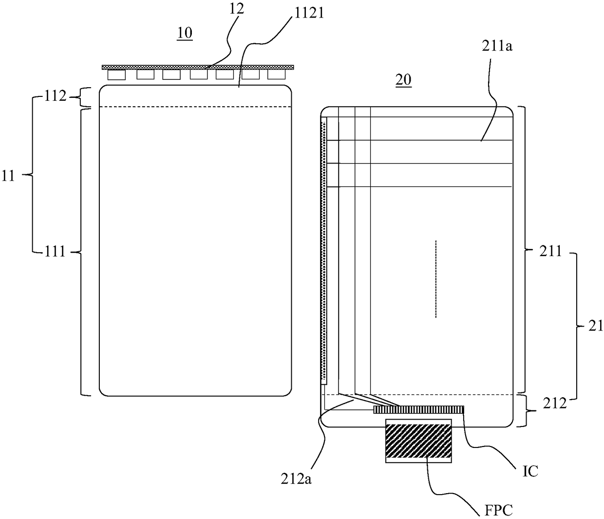
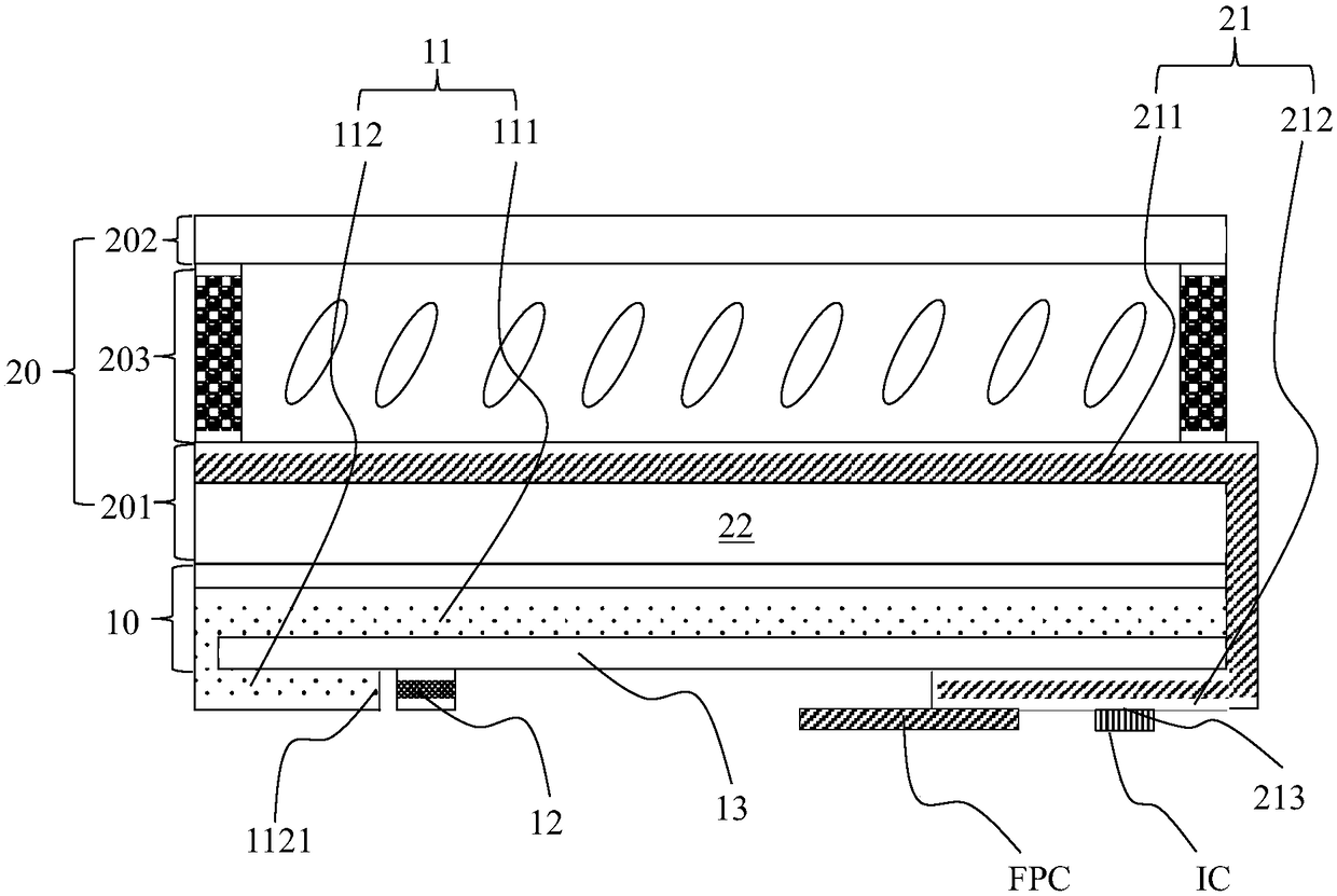
[0028] figure 1 A schematic structural diagram of a liquid crystal display device provided by an embodiment of the present invention, figure 2 for figure 1 The position comparison diagram of the backlight module and the liquid crystal display panel in the shown liquid crystal display device, image 3 for along figure 1 Schematic diagram of the cross-sectional structure of A1-A2. see figure 1 , figure 2 with image 3 The liquid crystal display device 100 includes: a liquid crystal display panel 20 and a ba...


PUM


Abstract

The invention discloses a liquid crystal display device. The device includes a liquid crystal display panel and a backlight module, a flexible substrate of the liquid crystal display panel includes aplanar region and a step region located on at least one side of the planar region, a light guide plate in the backlight module comprises a light emitting area and a bending area located on at least one side of the light emitting area, the light emitting area is disposed right against the planar area of the flexible substrate for performing a display function, the bending area and the step area arebent and attached to the surface of one side, away from a liquid crystal layer, of the backlight module, the problems that a frame area for accommodating the step region and a light source is required to be disposed on a liquid crystal display device, so that the frame width of the liquid crystal display device is large and the screen-to-body ratio is small are solved, and it is achieved that thestep area and the light source partially overlap with the display area of the liquid crystal display panel in a direction perpendicular to the backlight module, thereby reducing the frame width of the liquid crystal display device and increasing the screen-to-body ratio.

Description

technical field [0001] The invention relates to the field of display technology, in particular to a liquid crystal display device. Background technique [0002] The liquid crystal display device has the advantages of energy saving, thinness, and exquisite picture, and has been widely used in the field of display technology. With the continuous improvement of people's quality of life, people have higher and higher requirements for liquid crystal display devices, and liquid crystal display devices with narrow borders and full screens have become the focus of people's pursuit. [0003] The existing liquid crystal display device includes a liquid crystal display panel and a backlight module, wherein the liquid crystal display panel needs to be provided with a driving array and a control chip to provide driving voltage to the liquid crystal molecules in the display area. Wherein, the driving array is arranged in the display area, the control chip and the fan-out wiring electrica...

Claims


Application Information

Patent Timeline
Patent Type & Authority Applications(China)
IPC IPC(8): G02F1/1333G02F1/133G02F1/13357G02B6/00
CPCG02F1/133G02F1/133305G02F1/133605G02B6/0031G02B6/0055G02F1/134363G02F1/13452G02F1/133607G02F1/1333G02F1/1336G02B6/0011
Inventor 秦锋时成瑛夏志强
Owner SHANGHAI AVIC OPTOELECTRONICS
Why Eureka
Try Eureka