
Manufacturing method for printed circuit board, and printed circuit board

A technology for printed circuit boards and manufacturing methods, which is applied in the fields of printed circuit manufacturing, printed circuit, multi-layer circuit manufacturing, etc., and can solve the problems of whole board scrapping, high production cost, long delivery cycle, etc.

Inactive Publication Date: 2018-10-02
GUANGZHOU FASTPRINT CIRCUIT TECH +2
View PDF6 Cites 0 Cited by
  • Summary
  • Abstract
  • Description
  • Claims
  • Application Information

AI Technical Summary

Problems solved by technology

The printed circuit board products for wafer testing have the characteristics of high number of layers and high density. The center distance between the holes of the outer layer and the sub-outer layer is small and the number of layers is small. The center distance of the holes of the inner layer is large and the number of layers is high. It is made by multi-layer method, and multiple laminations not only lead to a long delivery cycle, but also put forward higher requirements on the heat resistance of the material. In addition, if one part is scrapped during the multiple lamination process, the entire board will be scrapped, and the production cost is high.

Method used


Image

  • Manufacturing method for printed circuit board, and printed circuit board
  • Manufacturing method for printed circuit board, and printed circuit board
  • Manufacturing method for printed circuit board, and printed circuit board

Examples


Embodiment Construction

[0024] In order to make the object, technical solution and advantages of the present invention clearer, the present invention will be further described in detail below in conjunction with the accompanying drawings and specific implementation methods. It should be understood that the specific embodiments described here are only used to explain the present invention, and do not limit the protection scope of the present invention.

[0025] It should be noted that when an element is referred to as being “fixed” to another element, it can be directly on the other element or there can also be an intervening element. When an element is referred to as being "connected to" another element, it can be directly connected to the other element or intervening elements may also be present. The terms "vertical," "horizontal," "left," "right," and similar expressions are used herein for purposes of illustration only and are not intended to represent the only embodiments.

[0026] Unless otherw...


PUM


Abstract

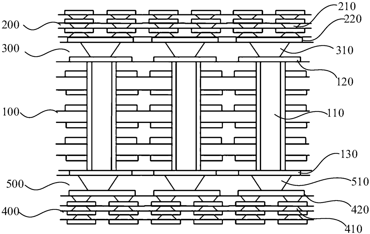
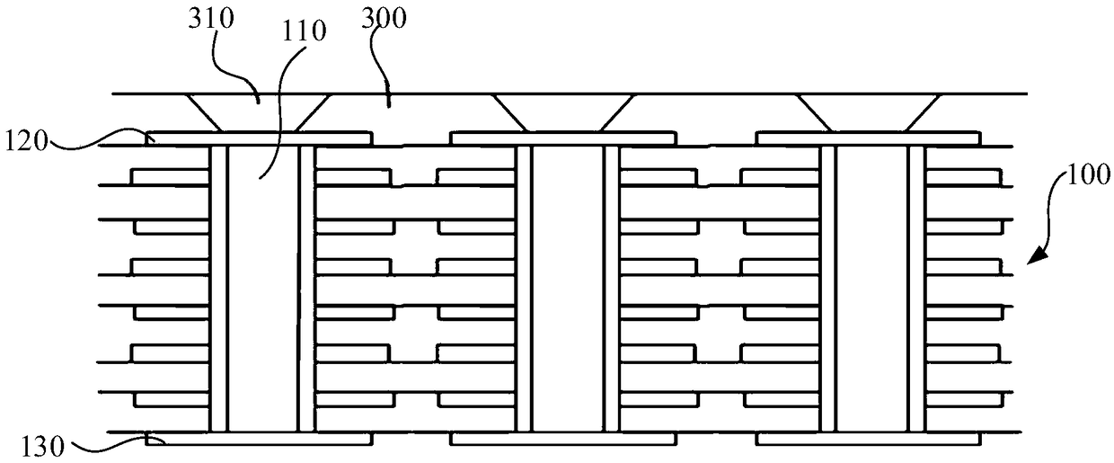
The invention relates to a manufacturing method for a printed circuit board, and the printed circuit board. The method comprises the steps: drilling a first prefabricated plate to obtain a first sub-board with a first connecting hole, and drilling a second prefabricated plate to obtain a second sub-board with a second connecting hole; pre-pressing a first bonding sheet on the first sub-board; forming a first via hole corresponding to the first connecting hole on the first bonding sheet; and performing the stitching of the first sub-board and the second sub-board through the first bonding sheet. The printed circuit board is fabricated through the above-described manufacturing method. According to the printed circuit board as described above, the connection holes in the printed circuit boardare divided according to the apertures and the center distances of the holes in the printed circuit board, sand the first and second sub-board which are different are separated out, and then the first sub-board and the second sub-board are connected by through the first bonding sheet including the first via hole.

Description

technical field [0001] The invention relates to the technical field of circuit boards, in particular to a method for manufacturing a printed circuit board and the printed circuit board. Background technique [0002] As electronic products continue to develop in light, thin, short, and small dimensions, the wiring density of corresponding printed circuit boards and electronic components is getting higher and higher, and the manufacturing process is becoming more and more difficult. The printed circuit board products for wafer testing have the characteristics of high number of layers and high density. The center distance between the holes of the outer layer and the sub-outer layer is small and the number of layers is small. The center distance of the holes of the inner layer is large and the number of layers is high. It is made by multi-layer method, and multiple laminations not only lead to a long delivery period, but also put forward higher requirements on the heat resistanc...

Claims


Application Information

Patent Timeline
Patent Type & Authority Applications(China)
IPC IPC(8): H05K3/46
CPCH05K3/4623
Inventor 陈丽琴廉泽阳李娟李艳国
Owner GUANGZHOU FASTPRINT CIRCUIT TECH
Learn More