Liquid crystal display panel, liquid crystal display device and manufacturing method for liquid crystal display panel

A technology of liquid crystal display panels and liquid crystal display devices, which is applied in nonlinear optics, instruments, optics, etc., and can solve problems such as inconvenient use, increased costs, and increased expenses

Active Publication Date: 2018-10-16
KUSN INFOVISION OPTOELECTRONICS
View PDF8 Cites 6 Cited by
  • Summary
  • Abstract
  • Description
  • Claims
  • Application Information

AI Technical Summary

Problems solved by technology

However, the method of coating the anti-blue light film layer on the glasses will increase additional expenses, and it needs to be worn at any time, which will increase the cost and be inconvenient to use; and the installation of the anti-blue light diffusion sheet will increase the manufacturing cost of the liquid crystal display device

Method used


Image

  • Liquid crystal display panel, liquid crystal display device and manufacturing method for liquid crystal display panel
  • Liquid crystal display panel, liquid crystal display device and manufacturing method for liquid crystal display panel
  • Liquid crystal display panel, liquid crystal display device and manufacturing method for liquid crystal display panel

Examples


no. 1 example

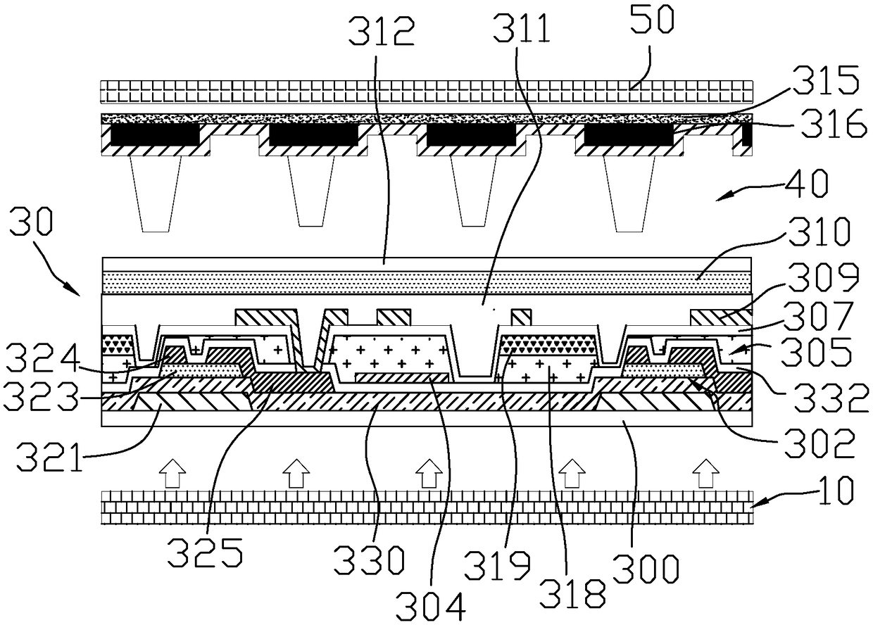
[0030] Such as figure 2 As shown, the liquid crystal display device provided in this embodiment includes a backlight module 10 and a liquid crystal display panel 30 . The liquid crystal display panel 30 is disposed on one side of the backlight module 10 .

[0031] The liquid crystal display panel 30 includes a first substrate, a second substrate and a liquid crystal layer 40 disposed between them. The first substrate includes a substrate 300, a thin film transistor 302 stacked on the substrate 300, and a first conductive layer 304 in sequence. , color resist layer 305 , insulating layer 307 , second conductive layer 309 , first protective layer 311 , first polarizer 310 and second protective layer 312 . The first conductive layer 302 is insulated from the second conductive layer 304 , the first conductive layer 302 can be specifically formed as a pixel electrode, and the second conductive layer 304 can be specifically formed as a common electrode.

[0032] In this embodimen...

no. 2 example

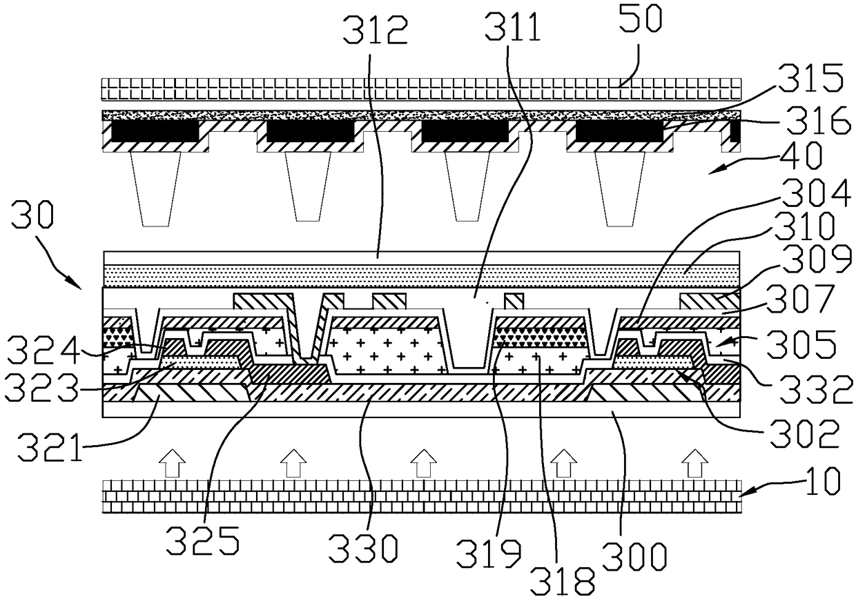
[0042] Such as image 3As shown, the liquid crystal display device provided in this embodiment includes a backlight module 10 and a liquid crystal display panel 30 . The liquid crystal display panel 30 is disposed on one side of the backlight module 10 .

[0043] The difference between the liquid crystal display device of this embodiment and the liquid crystal display device of the first embodiment lies in that the position of the first conductive layer 304 in the liquid crystal display panel 30 is different.

[0044] In this embodiment, the liquid crystal display panel 30 includes a substrate 300, a thin film transistor 302, a color resist layer 305, a first conductive layer 304, an insulating layer 307, a second conductive layer 309, a first protective layer 311, a A polarizer 310 and a second protection layer 312 . The first conductive layer 302 is insulated from the second conductive layer 309 , the first conductive layer 302 can be specifically formed as a pixel electro...

no. 3 example

[0055] Such as Figure 4 As shown, the manufacturing method of the liquid crystal display panel according to the third embodiment of the present invention is: forming a first substrate, a second substrate and a liquid crystal layer, and disposing the liquid crystal layer 40 between the first substrate and the second substrate.

[0056] Specifically, the method for forming the first substrate includes:

[0057] S11 , providing a substrate 300 . The substrate 300 is a glass substrate or a transparent plastic substrate.

[0058] S13 , forming a thin film transistor 302 on the substrate 300 , where the thin film transistor 302 is located on a side of the substrate 300 close to the liquid crystal layer 40 . There are multiple thin film transistors arranged in an array on the substrate 300 . Specifically, when forming a thin film transistor, the gate 321 is first formed on the substrate 300, the first passivation layer 330 covering the gate 321 is formed on the gate 321, the semi...


PUM


Abstract

The invention discloses a liquid crystal display panel, a liquid crystal display device and a manufacturing method for the liquid crystal display panel. The liquid crystal display panel comprises a first substrate, a second substrate and a liquid crystal layer arranged between the first substrate and the second substrate, the first substrate comprises a substratum and a thin film transistor arranged on the substratum, a color resistance layer is further arranged on the first substrate, the color resistance layer comprises a blue color resistor, a red resistor and a green color resistor, and quantum dot layers are stacked at one side, away from the substratum, of the blue resistor. According to the liquid crystal display panel, the liquid crystal display device and the manufacturing methodfor the liquid crystal display panel, it is due to the fact that the quantum dot layers are arranged on the corresponding position of the blue resistor, quantum dots on the quantum dot layer are motivated by a backlight module, high-energy blue light can be eliminated, the effect of protecting eyesight is achieved, and melatonin secretion cannot be affected; in addition, it is only required that the quantum dot layers are additionally arranged on the original multicolor resistance layer, the multicolor resistance layer does not need to be changed excessively, and increasing extra expenses is not needed.

Description

technical field [0001] The invention relates to the field of liquid crystal display, in particular to a liquid crystal display panel, a liquid crystal display device and a method for manufacturing a liquid crystal display panel. Background technique [0002] Currently, liquid crystal display devices are widely used in various electronic products. The liquid crystal display device includes a liquid crystal display panel and a backlight module. Such as figure 1 As shown, a liquid crystal display device includes a liquid crystal display panel and a backlight module 91. The liquid crystal display panel includes an array substrate 92, a liquid crystal layer 94, and a color filter substrate 95. The liquid crystal layer 94 is arranged on the array substrate 92 and the color filter substrate 95. between. The thin film transistors of the array substrate 92 are disposed on the first substrate 96 , and the color resist layer of the color filter substrate 95 is disposed on the second...

Claims


Application Information

Patent Timeline
Patent Type & Authority Applications(China)
IPC IPC(8): G02F1/1335G02F1/13357
CPCG02F1/133514G02F1/1336G02F1/133614
Inventor 刘茜朱梦青何淑慧陈尧
Owner KUSN INFOVISION OPTOELECTRONICS
Why Eureka
Try Eureka