Liquid crystal display panel, liquid crystal display device, and method for manufacturing liquid crystal display panel
A liquid crystal display panel and liquid crystal display device technology, applied in the direction of instruments, nonlinear optics, optics, etc., can solve the problems of increasing the manufacturing cost of liquid crystal display devices, increasing costs, increasing expenses, etc., and achieve the effect of protecting eyesight
- Summary
- Abstract
- Description
- Claims
- Application Information
AI Technical Summary
Problems solved by technology
Method used
Image
Examples
no. 1 example
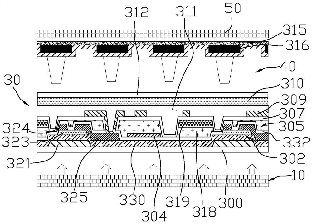
[0030] like figure 2 As shown, the liquid crystal display device provided in this embodiment includes a backlight module 10 and a liquid crystal display panel 30 . The liquid crystal display panel 30 is disposed on one side of the backlight module 10 .
[0031] The liquid crystal display panel 30 includes a first substrate, a second substrate, and a liquid crystal layer 40 disposed therebetween. The first substrate includes a substrate 300 , a thin film transistor 302 and a first conductive layer 304 stacked on the substrate 300 in sequence. , a color resist layer 305 , an insulating layer 307 , a second conductive layer 309 , a first protective layer 311 , a first polarizer 310 and a second protective layer 312 . The first conductive layer 304 and the second conductive layer 309 are spaced and insulated, the first conductive layer 304 can be formed as a common electrode, and the second conductive layer 309 can be formed as a pixel electrode.
[0032] In this embodiment, th...
no. 2 example
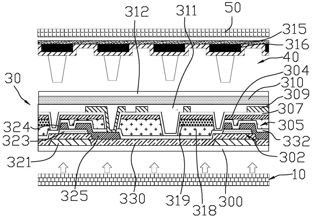
[0042] like image 3As shown, the liquid crystal display device provided in this embodiment includes a backlight module 10 and a liquid crystal display panel 30 . The liquid crystal display panel 30 is disposed on one side of the backlight module 10 .
[0043] The difference between the liquid crystal display device of this embodiment and the liquid crystal display device of the first embodiment is that the positions of the first conductive layers 304 in the liquid crystal display panel 30 are different.
[0044] In this embodiment, the liquid crystal display panel 30 includes a substrate 300, a thin film transistor 302, a color resist layer 305, a first conductive layer 304, an insulating layer 307, a second conductive layer 309, a first protective layer 311, a first conductive layer 309, a first protective layer 311, a A polarizer 310 and a second protective layer 312 . The first conductive layer 304 and the second conductive layer 309 are spaced and insulated, the first c...
no. 3 example
[0055] like Figure 4 As shown, the method for manufacturing a liquid crystal display panel according to the third embodiment of the present invention is as follows: forming a first substrate, a second substrate and a liquid crystal layer, and disposing the liquid crystal layer 40 between the first substrate and the second substrate.
[0056] Specifically, the method of forming the first substrate includes:
[0057] S11, the substrate 300 is provided. The substrate 300 is a glass substrate or a transparent plastic substrate.
[0058] S13 , forming a thin film transistor 302 on the substrate 300 , and the thin film transistor 302 is located on the side of the substrate 300 close to the liquid crystal layer 40 . A plurality of thin film transistors are arranged on the substrate 300 in an array. Specifically, when forming a thin film transistor, a gate electrode 321 is first formed on the substrate 300, a first passivation layer 330 covering the gate electrode 321 is formed on...
PUM
 Abstract
Description
Claims
Application Information


