Storage component testing method and device

A technology of storage components and test methods, applied in static memory, instruments, etc., can solve problems such as single test method, inability to provide coverage, address traversal sequence, read and write operation sequence address space cannot be flexibly configured, etc. Simplify configuration steps and improve test coverage

Active Publication Date: 2018-10-16
SANECHIPS TECH CO LTD
View PDF4 Cites 4 Cited by
  • Summary
  • Abstract
  • Description
  • Claims
  • Application Information

AI Technical Summary

Problems solved by technology

[0002] In the existing multi-chip package dynamic random access memory (DRAM, Dynamic Random Access Memory) built-in self-test method, the address traversal order, read and write operation order, address space, etc. cannot be flexibly configured, and the test vectors that can be combined It is very simple and cannot provide sufficient coverage; for example, Synopsis's double-rate synchronous dynamic random access memory physical layer (DDR PHY, Double Data Rate synchronous dynamic random access memory PHYsical layer), which provides DRAM built-in self-test (BIST, Build In Self-Test), the address space of a test is only 2Mbit, and only 8 data lines (DQ) can be tested each time; for the current 1Gbit or larger DRAM, the DRAM with a bit width of 32 bits needs to be configured multiple times ; Moreover, the read and write sequence of DDR PHY can only provide the operation sequence of increasing the Y address direction and writing first and then reading, and the test method is relatively simple

Method used


Image

  • Storage component testing method and device
  • Storage component testing method and device
  • Storage component testing method and device

Examples


Embodiment Construction

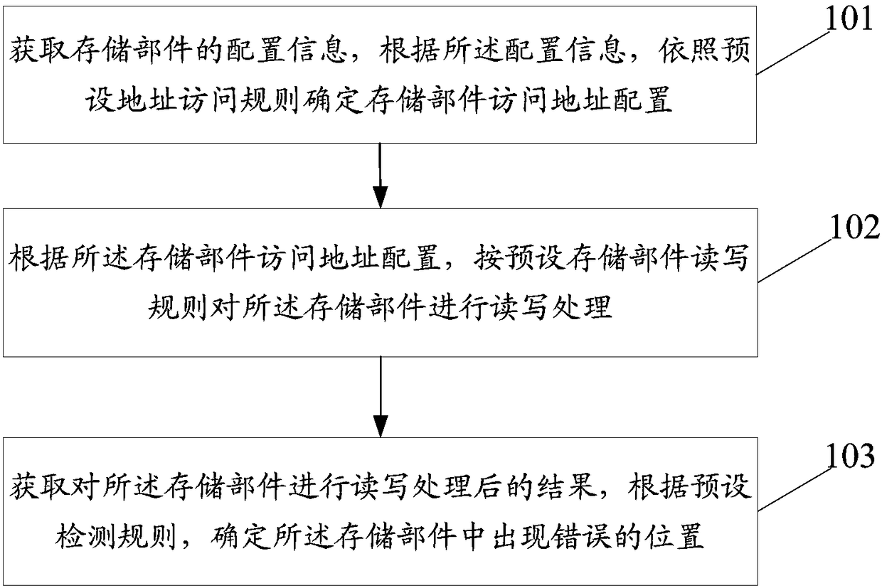
[0043] In the embodiment of the present invention, the configuration information of the storage component is acquired, and according to the configuration information, the storage component access address configuration is determined according to the preset address access rules; according to the storage component access address configuration, the storage component is read and written according to the preset storage component access address configuration The storage component performs read and write processing; obtains the result of the storage component after the read and write processing, and determines the location of the error in the storage component according to a preset detection rule.

[0044] The present invention will be described in further detail below in conjunction with the examples.

[0045] The storage component testing method provided by the embodiment of the present invention, such as figure 1 As shown, the method includes:

[0046] Step 101: Obtain the configu...


PUM


Abstract

The invention discloses a storage component testing method. According to the method, configuration information of a storage component is acquired, and storage component access address configuration isdetermined according to the configuration information and preset address access rules; read-write processing is performed on the storage component according to the storage component access address configuration and preset storage component read-write rules; and a result obtained after read-write processing of the storage component is acquired, and the position of an error in the storage componentis determined according to preset detection rules. The invention furthermore discloses a storage component testing device.

Description

technical field [0001] The invention relates to a multi-chip packaging and testing technology, in particular to a storage component testing method and device. Background technique [0002] In the existing multi-chip package dynamic random access memory (DRAM, Dynamic Random Access Memory) built-in self-test method, the address traversal order, read and write operation order, address space, etc. cannot be flexibly configured, and the test vectors that can be combined It is very simple and cannot provide sufficient coverage; for example, Synopsis's double-rate synchronous dynamic random access memory physical layer (DDR PHY, Double Data Rate synchronous dynamic random access memory PHYsical layer), which provides DRAM built-in self-test (BIST, Build In Self-Test), the address space of a test is only 2Mbit, and only 8 data lines (DQ) can be tested each time; for the current 1Gbit or larger DRAM, the DRAM with a bit width of 32 bits needs to be configured multiple times ; Moreo...

Claims


Application Information

Patent Timeline
IPC IPC(8): G11C29/18G11C29/14G11C29/36G11C29/44G11C29/12
CPCG11C29/12G11C29/14G11C29/18G11C29/36G11C29/44G11C2029/1208G11C2029/4402
Inventor 李光耀吕玲
Owner SANECHIPS TECH CO LTD
Why Eureka
Try Eureka