Low-temperature electronic interconnection material, preparation method thereof and low-temperature electronic interconnection method
An electronic interconnection and low-temperature technology, which is applied in the direction of circuits, electrical components, and electrical solid devices, can solve limitations and other problems, and achieve the effects of densification, low-temperature interconnection, and excellent low-temperature interconnection characteristics
- Summary
- Abstract
- Description
- Claims
- Application Information
AI Technical Summary
Problems solved by technology
Method used
Image

Examples
Embodiment 1
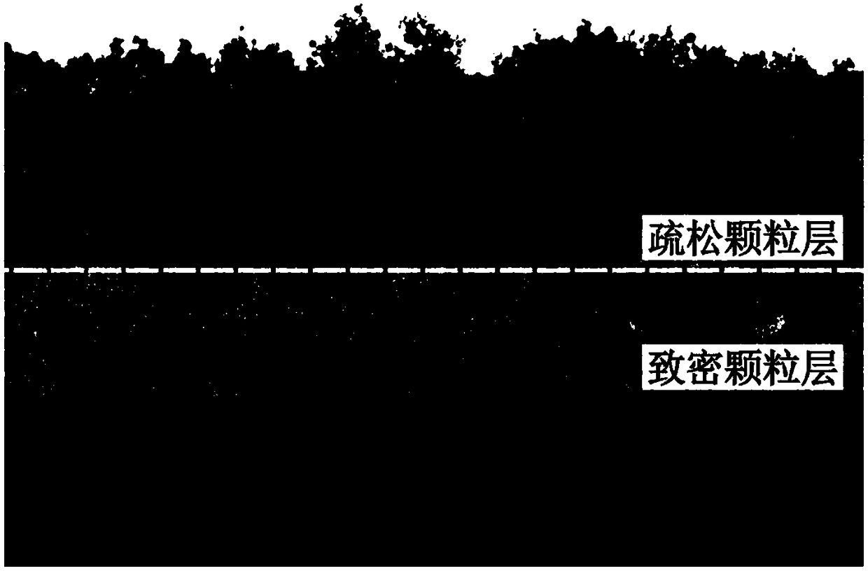
[0053] The present embodiment provides a kind of preparation method of dense-loose binary structure particle layer, it comprises the following steps:
[0054] Using laser deposition technology, using high-purity silver target material, deposit a dense particle layer on the surface of the parts to be connected. The process parameters used for deposition are: target base distance 37mm, laser average power 100W, deposition pressure 0.5Pa, deposition time 20min. A dense silver particle layer with a thickness of 22 μm, a density of 90%, and an average particle size of 500 nm was obtained on the surface of the parts to be connected.
[0055] Then, a loose granular layer is deposited on the surface of the dense granular layer of the parts to be connected. The process parameters used for deposition are: target base distance 50mm, average laser power 100W, deposition pressure 1400Pa, deposition time 8min. Obtain a silver loose particle layer with a thickness of 80 μm, a density of 60%,...
Embodiment 2
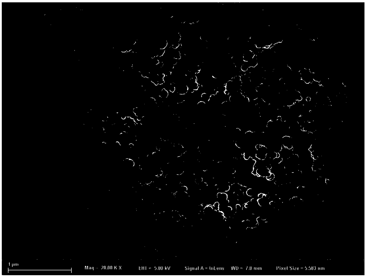
[0057] The present embodiment provides the preparation method of silver dense grain layer, and it comprises the following steps:
[0058] Using laser deposition technology, using high-purity silver targets, deposit a dense particle layer on the surface of the parts to be connected. The process parameters used for deposition are: target base distance 90mm, laser average power 15W, deposition pressure 10 -3 Pa, deposition time 30min. On the surface of the parts to be connected, a silver dense particle layer with a thickness of 5 μm, a density of 92%, and an average particle size of 120 nm is obtained, and its surface appearance is as follows: figure 2 shown.
Embodiment 3
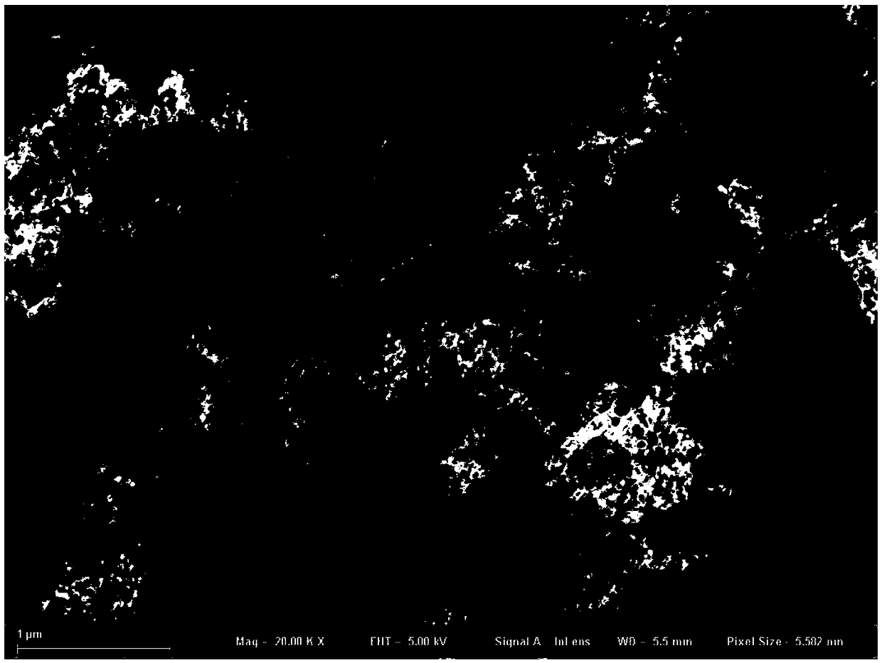
[0060] The present embodiment provides the preparation method of silver loose granular layer, and it comprises the following steps:
[0061] Using laser deposition technology, using high-purity silver target material, deposit a loose particle layer on the surface of the parts to be connected. The process parameters used for deposition are: target base distance 67mm, average laser power 25W, deposition pressure 1500Pa, deposition time 10min. Obtain a silver loose particle layer with a thickness of 10 μm, a density of 35%, and an average particle size of 40 nm on the surface of the part to be connected, and its surface appearance is as follows: image 3 shown.
PUM
| Property | Measurement | Unit |
|---|---|---|
| Size | aaaaa | aaaaa |
| Thickness | aaaaa | aaaaa |
| The average particle size | aaaaa | aaaaa |
Abstract
Description
Claims
Application Information
 - R&D
- Intellectual Property
- Life Sciences
- Materials
- Tech Scout
- Unparalleled Data Quality
- Higher Quality Content
- 60% Fewer Hallucinations
Browse by: Latest US Patents, China's latest patents, Technical Efficacy Thesaurus, Application Domain, Technology Topic, Popular Technical Reports.
© 2025 PatSnap. All rights reserved.Legal|Privacy policy|Modern Slavery Act Transparency Statement|Sitemap|About US| Contact US: help@patsnap.com