Method for checking detection accuracy of defect detecting machine and product wafer

A technology of detection accuracy and calibration method, applied in semiconductor/solid state device testing/measurement, electrical components, electric solid state devices, etc., can solve the problem of high calibration cost, increase calibration frequency, reduce calibration cost, guarantee The effect of accuracy

Active Publication Date: 2018-10-23
SEMICON MFG INT (SHANGHAI) CORP +1
View PDF3 Cites 1 Cited by
  • Summary
  • Abstract
  • Description
  • Claims
  • Application Information

AI Technical Summary

Problems solved by technology

[0006] The purpose of the present invention is to provide a method for verifying the detection accuracy of a defect detection machine and a product wafer, so as to solve the problem in the prior art that the verification cost of verifying the detection accuracy of a defect detection machine is very high

Method used


Image

  • Method for checking detection accuracy of defect detecting machine and product wafer
  • Method for checking detection accuracy of defect detecting machine and product wafer
  • Method for checking detection accuracy of defect detecting machine and product wafer

Examples


Embodiment Construction

[0031] The method for verifying the detection accuracy of the defect detection machine and the product wafer proposed by the present invention will be further described in detail below in conjunction with the accompanying drawings and specific embodiments. Advantages and features of the present invention will be apparent from the following description and claims. It should be noted that all the drawings are in a very simplified form and use imprecise scales, and are only used to facilitate and clearly assist the purpose of illustrating the embodiments of the present invention. In addition, the structures shown in the drawings are often a part of the actual structures. In particular, each drawing needs to display different emphases, and sometimes uses different scales.

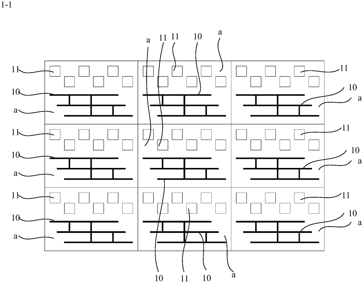
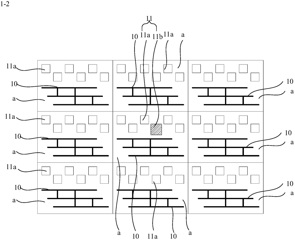
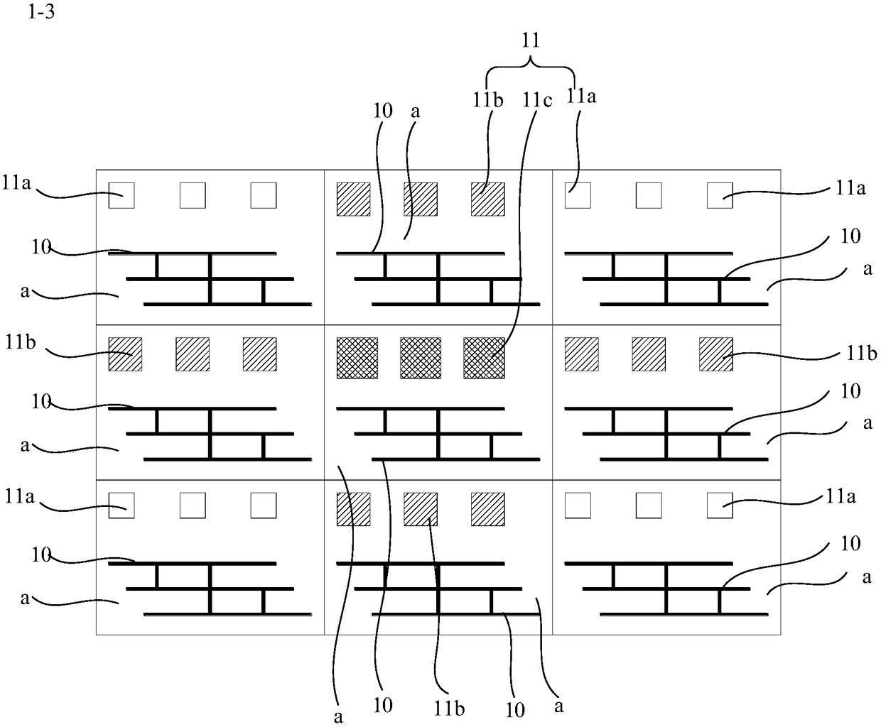
[0032] The method for verifying the detection accuracy of the defect detection machine provided in the embodiment of the present application is mainly realized based on the product wafer. Therefore, in the emb...


PUM


Abstract

The invention provides a method for checking the detection accuracy of a defect detecting machine and a product wafer. According to the invention, a virtual structure in the product wafer is obtained,and the detection accuracy of the defect detecting machine is obtained according to data of the obtained virtual structure, so that a standard wafer is not required to be used, and thus the checkingcost of performing checking on the detection accuracy of the defect detecting machine can be reduced. Furthermore, the product wafer in the manufacturing process is adopted, and the product wafer itself has very high quality requirements on the aspects of cleanliness and the like, so that there are basically no problems such as contamination, and thus the accuracy of the checking result can also be improved.

Description

technical field [0001] The invention relates to the technical field of integrated circuits, in particular to a method for verifying the detection accuracy of a defect detection machine and a product wafer. Background technique [0002] In the integrated circuit manufacturing process, as time goes by, different conditions will appear on the equipment machine, such as unstable performance, failure, etc. In order to be able to monitor the equipment machine in time and know whether its performance is deviated, it is necessary to use the defect inspection tool (Defect inspection tool) to detect the defects of the product wafers manufactured by the equipment machine, so as to judge the performance of the equipment machine . With the continuous improvement of integrated circuit manufacturing technology and the increasing demand for production capacity, defect detection machines play an extremely important role in the monitoring of equipment machine performance and product wafer de...

Claims


Application Information

Patent Timeline
Patent Type & Authority Applications(China)
IPC IPC(8): H01L21/66H01L23/544
CPCH01L22/12H01L22/20H01L22/30
Inventor 姚笛方鑫陈思安张珏
Owner SEMICON MFG INT (SHANGHAI) CORP
Why Eureka
Try Eureka