Film photovoltaic device and manufacturing method thereof

A thin-film photovoltaic and device technology, which is applied in semiconductor/solid-state device manufacturing, photovoltaic power generation, electric solid-state devices, etc., can solve the problems of low parallel resistance, low photocurrent, high series resistance, etc., to reduce potential barriers and increase electrical coupling , Improve the effect of electrical performance

Active Publication Date: 2018-10-23
TCL CORPORATION
View PDF3 Cites 0 Cited by
  • Summary
  • Abstract
  • Description
  • Claims
  • Application Information

AI Technical Summary

Problems solved by technology

[0006] In view of the above-mentioned deficiencies in the prior art, the object of the present invention is to provide a thin film photovoltaic device and a preparation method thereof, aiming at solving the problem that the existing thin film photovoltaic device has a relatively high series resistance and a low parallel resistance, resulting in relatively low internal photocurrent. low problem

Method used


Image

  • Film photovoltaic device and manufacturing method thereof
  • Film photovoltaic device and manufacturing method thereof
  • Film photovoltaic device and manufacturing method thereof

Examples


Embodiment Construction

[0036] The present invention provides a thin-film photovoltaic device and its preparation method. In order to make the purpose, technical solution and effect of the present invention clearer and clearer, the present invention will be further described in detail below. It should be understood that the specific embodiments described here are only used to explain the present invention, not to limit the present invention.

[0037] A preferred embodiment of the preparation method of a thin film photovoltaic device of the present invention, including:

[0038] Step A, depositing a light absorbing layer on the first electrode;

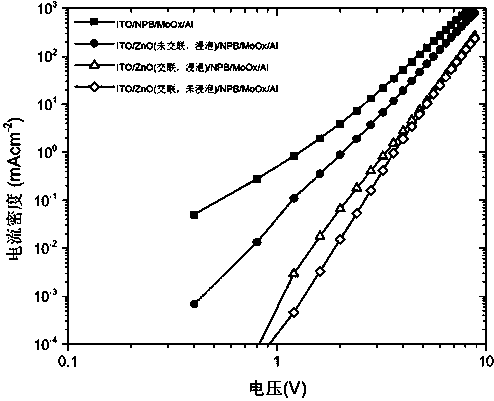
[0039] Step B, depositing an electron extraction layer on the light-absorbing layer, the material of the electron extraction layer is a cross-linked nano-particle film formed by cross-linking the nano-particle film;

[0040] Step C, evaporating a second electrode on the electron extraction layer to obtain a thin film photovoltaic device.

[0041] Specifical...


PUM


Abstract

The invention discloses a film photovoltaic device and a manufacturing method thereof. The method comprises the following steps of step A, depositing a light absorption layer on a first electrode; step B, depositing an electronic extraction layer on the light absorption layer, wherein the material of the electronic extraction layer is a cross-linked nano-particle film formed through carrying out crosslinking treatment on a nanoparticle film; and step C, evaporating a second electrode on the electronic extraction layer and acquiring the film photovoltaic device. In the invention, the acquired cross-linked nano-particle film is applied in the film photovoltaic device manufactured through a solution method, a parallel resistance in the photovoltaic device can be greatly increased and a seriesresistance in the photovoltaic device is reduced so that the light current of a fill factor in the film photovoltaic device is increased, and then the photoelectric conversion efficiency of the device is improved.

Description

technical field [0001] The invention relates to the field of photovoltaic devices, in particular to a thin-film photovoltaic device and a preparation method thereof. Background technique [0002] Photovoltaic devices refer to devices that can directly convert light energy into electrical energy by using the photovoltaic effect at the semiconductor interface. [0003] In the process of preparing photovoltaic devices by solution method, oxide nanoparticles are one of the important solutions for forming corresponding oxide films, mainly because oxide nanoparticles (or spherical oxide nanocrystals) have good crystallinity, which ensures On the other hand, due to the good self-assembly of oxide nanoparticles into films, low-cost coating preparation processes can be applied. Common oxide nanoparticles include zinc oxide (ZnO x ) nanoparticles, titanium oxide (TiO x ) Nanoparticles, etc., the nanoparticle film is usually used in thin film photovoltaic devices as a semiconductor ...

Claims


Application Information

Patent Timeline
Patent Type & Authority Applications(China)
IPC IPC(8): H01L31/18H01L51/42H01L51/48H01L51/46
CPCH01L31/0216H01L31/0445H01L31/1804H01L31/1828H10K30/00H10K2102/00Y02E10/549Y02E10/543Y02E10/547Y02P70/50
Inventor 陈崧钱磊杨一行曹蔚然向超宇
Owner TCL CORPORATION
Why Eureka
Try Eureka