

Display device, manufacturing method thereof, and display device
A display device and electrode packaging technology, which is applied in semiconductor/solid-state device manufacturing, electric solid-state devices, semiconductor devices, etc., can solve problems such as low utilization rate, large film-forming area, and complicated process, so as to save usage and reduce costs , Improve the effect of comprehensive mechanical properties
Active Publication Date: 2019-10-01
BOE TECH GRP CO LTD +1
View PDF5 Cites 0 Cited by
- Summary
- Abstract
- Description
- Claims
- Application Information
AI Technical Summary
Problems solved by technology
The general OLED manufacturing process is to deposit the anode, hole injection layer, light-emitting layer, and cathode in sequence, and a diaphragm of a specific film quality must be specially set between individual pixels to separate them, and then the OLED is packaged, which is a complicated process; and the packaging material is coated. During the coating process, the film forming area is large and the utilization rate is low
Method used
View moreImage
Smart ImageViewing Examples

Examples
Embodiment Construction
Login to View More PUM
 Abstract
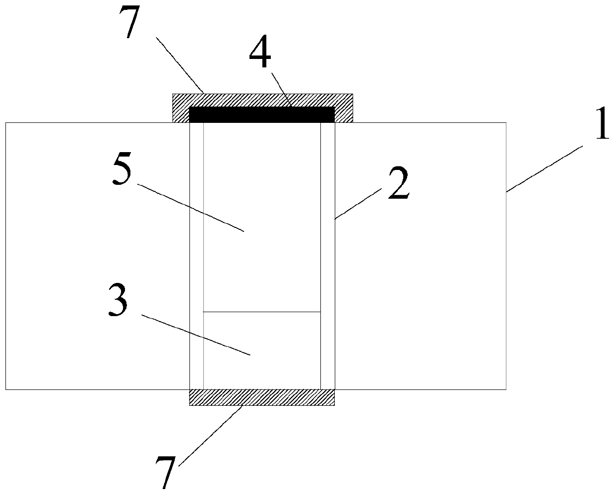
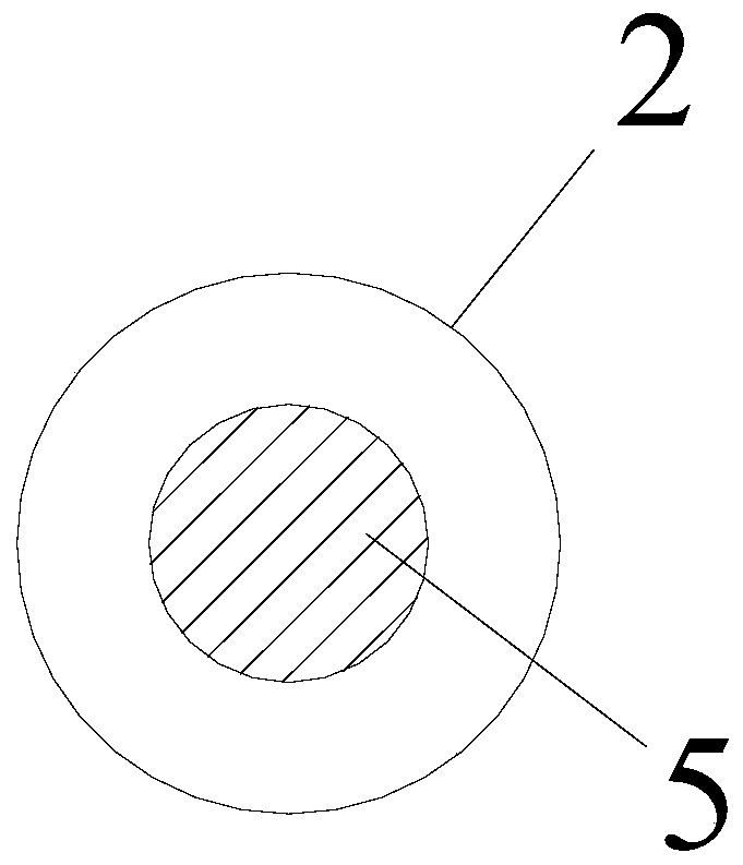
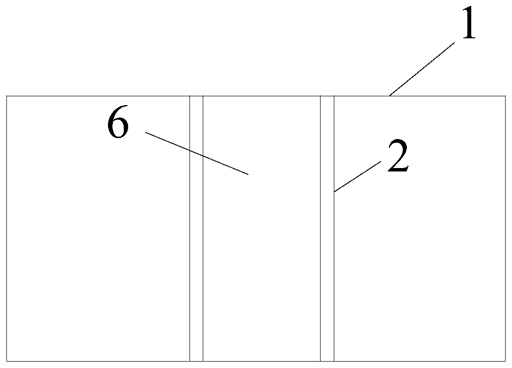
The invention discloses a display device, a preparation method thereof, and a display device. The display device includes a carrier, on which nanotubes are arranged, and inside the nanotubes are provided accommodation chambers with openings at both ends. A first electrode and a luminescent layer are provided, the first electrode encapsulates one end opening of the accommodating cavity, and the end opening of the accommodating cavity away from the first electrode is encapsulated by a second electrode, and the luminescent layer is located in the second electrode. Between the first electrode and the second electrode; the display device realizes self-encapsulation, which saves the usage of packaging materials to the greatest extent and reduces the cost.
Description
technical field The invention relates to the display field, in particular to a display device, a manufacturing method thereof, and a display device. Background technique Organic light-emitting diodes, that is, OLEDs, have excellent characteristics such as ultra-thin, low power consumption, fast response speed, self-illumination, high contrast, wide viewing angle, and can be used for flexible panels. The general OLED manufacturing process is to deposit the anode, hole injection layer, light-emitting layer, and cathode in sequence, and a diaphragm of a specific film quality must be specially set between individual pixels to separate them, and then the OLED is packaged, which is a complicated process; and the packaging material is coated. During the covering process, the film forming area is large and the utilization rate is low. Contents of the invention In order to solve the above technical problems, the present invention provides a display device, a manufacturing method ...
Claims
Login to View More Application Information
Patent Timeline
 Patent Type & AuthorityPatents(China)
IPC IPC(8): H01L51/52H01L51/56B82Y30/00
CPCB82Y30/00H10K71/00H10K59/873H10K50/182H10K2102/3023H10K50/84
Inventor董晓楠谌伟吴旭黄中浩赵永亮
OwnerBOE TECH GRP CO LTD