
Silicon wafer clamp, detection device and detection method thereof

A technology for detecting devices and silicon wafers, which is applied in the direction of measuring devices, workpiece clamping devices, and optical testing for flaws/defects. Guaranteed accuracy and high detection accuracy

Active Publication Date: 2020-11-20
ZING SEMICON CORP
View PDF8 Cites 0 Cited by
  • Summary
  • Abstract
  • Description
  • Claims
  • Application Information

AI Technical Summary

Problems solved by technology

[0005] The object of the present invention is to provide a silicon wafer clamp, a detection device and a detection method thereof, so as to solve the problems that some edges of the silicon wafer cannot be detected and the detection efficiency is low in the prior art

Method used


Image

  • Silicon wafer clamp, detection device and detection method thereof
  • Silicon wafer clamp, detection device and detection method thereof
  • Silicon wafer clamp, detection device and detection method thereof

Examples


Embodiment Construction

[0051] The following will be combined with figure 2 To attach Figure 7 , and the specific embodiments describe the silicon wafer holder, detection device and detection method proposed by the present invention in more detail. Advantages and features of the present invention will be apparent from the following description and claims. It should be noted that all the drawings are in a very simplified form and use imprecise scales, and are only used to facilitate and clearly assist the purpose of illustrating the embodiments of the present invention.

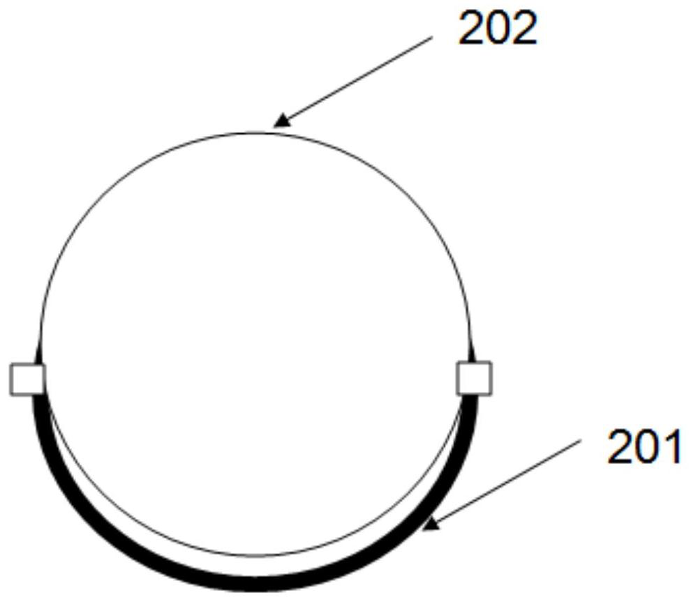
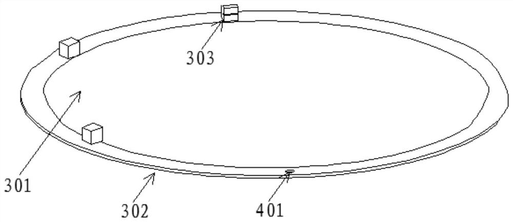
[0052] image 3 A structural schematic diagram of a silicon wafer clip provided in an embodiment of the present invention, such as image 3As shown, the wafer clip includes a clip 302 and a holder 303 . Wherein, the clip 302 is connected with the holder 303 and jointly forms an accommodating space 301, and when a silicon wafer is accommodated in the accommodating space 301 and fixed with the silicon wafer clip, through the acco...


PUM


Abstract

The invention provides a silicon wafer clamp, a detection device and a detection method thereof. The silicon wafer clamp comprises a clamping sheet and a clamper which is connected to the clamping sheet, wherein the clamping sheet and the clamper form an accommodating space; a silicon wafer is combined with the accommodating space, and all surfaces of the silicon wafer can be observed through theaccommodating space. The detecting device comprises the silicon wafer clamp, and a handheld rod which is connected to the silicon wafer clamp; the silicon wafer clamp is driven to move through the handheld rod, so as to realize the detection of all surfaces of the silicon wafer. The detecting method comprises the step of overturning the silicon wafer clamp through the handheld rod so as to detectthe upper surface, the lower surface and the side surface of the silicon wafer on the silicon wafer clamp. Due to the adoption of the silicon wafer clamp, the detecting device and the detecting methodthereof, all side edges of the silicon wafer can be detected; meanwhile, the detecting accuracy can be improved when an operator is unskilled.

Description

technical field [0001] The invention relates to the field of semiconductor manufacturing, in particular to a silicon wafer clamp, a detection device and a detection method thereof. Background technique [0002] With the continuous reduction of semiconductor feature size, the semiconductor industry has higher and higher requirements for surface defects of 12-inch silicon wafers. That is to say, the semiconductor industry not only has higher and higher requirements for the defects on the front side of silicon wafers, but also has more and more stringent requirements on the back side defects and edge defects of silicon wafers. These defects include, for example, stains, scratches, and gaps on the edge of the silicon wafer, etc., and these defects are usually found by human inspection devices. [0003] figure 1 It is a structural schematic diagram of an existing detection device, figure 2 It is a schematic diagram of the structure of an existing silicon chip sandwiched by a ...

Claims


Application Information

Patent Timeline
Patent Type & Authority Patents(China)
IPC IPC(8): G01N21/88B25B11/00
CPCB25B11/00G01N21/8803
Inventor 汪燕刘源
Owner ZING SEMICON CORP
Features
  • Generate Ideas
  • Intellectual Property
  • Life Sciences
  • Materials
  • Tech Scout
  • Unparalleled Data Quality
  • Higher Quality Content
  • 60% Fewer Hallucinations
Learn More