

LED lighting device and manufacture method thereof
A technology for LED lighting and manufacturing methods, applied in electrical components, electrical solid devices, circuits, etc., can solve problems such as unfavorable package reliability, LED pad damage, etc., to save solder, prevent warpage, and prevent temperature differences. Effect
- Summary
- Abstract
- Description
- Claims
- Application Information
AI Technical Summary
Problems solved by technology
Method used
Image

Examples
Embodiment Construction
[0026] see Figure 2-8 , the manufacturing method of the LED lighting device of the present invention, comprising:
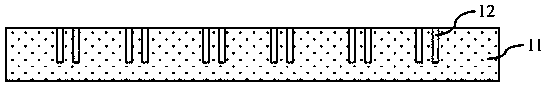
[0027] (1) Reference figure 2 , providing a ceramic substrate 11, the ceramic substrate 11 has an opposite first surface and a second surface, and a plurality of annular blind holes 12 are formed on the first surface by laser groove technology;
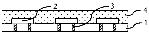
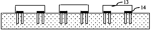
[0028] (2) Reference image 3 with 4 , a plurality of LED chips 13 are distributed on the first surface with their pads 14 facing the first surface, the pads 14 correspond to the annular blind holes 12 one by one, and the LED chips 13 completely cover the annular blind hole 12, and form a plastic sealing layer 15 on the first surface, and the plastic sealing layer 15 completely covers the LED chip 13;
[0029] (3) Reference Figure 5 , thinning the second surface by mechanical polishing until the annular blind hole 12 is exposed;
[0030] (4) Reference Image 6 , taking out a plurality of ceramic pillars 17 in t...
PUM
 Abstract
Description
Claims
Application Information