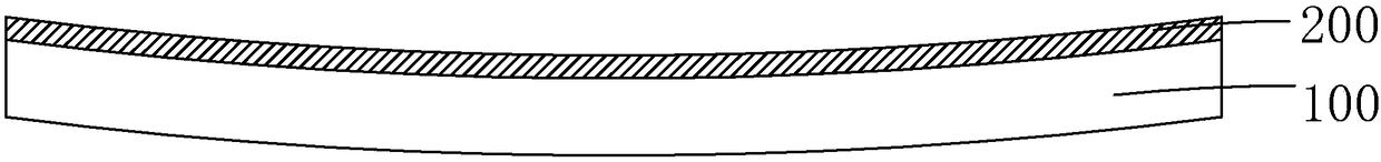
Film forming method for reducing warpage of mother board
A film-forming method and motherboard technology, applied in nonlinear optics, instruments, optics, etc., can solve problems such as increased risk of fragmentation and warping of glass motherboard 100, and achieve the goals of reducing the risk of fragmentation, releasing stress, and reducing warpage Effect
- Summary
- Abstract
- Description
- Claims
- Application Information
AI Technical Summary
Problems solved by technology
Method used
Image

Examples
Embodiment Construction
[0029] In order to further illustrate the technical means adopted by the present invention and its effects, the following describes in detail the preferred embodiments of the present invention and the accompanying drawings.
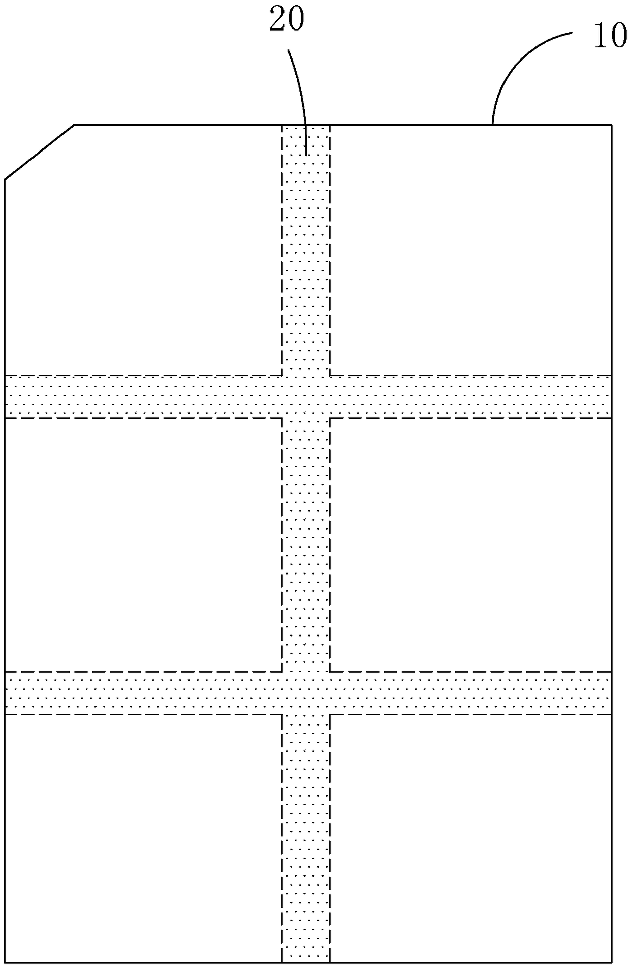
[0030] See Image 6 , The present invention provides a film forming method for reducing the warpage of a mother board, which includes the following steps:
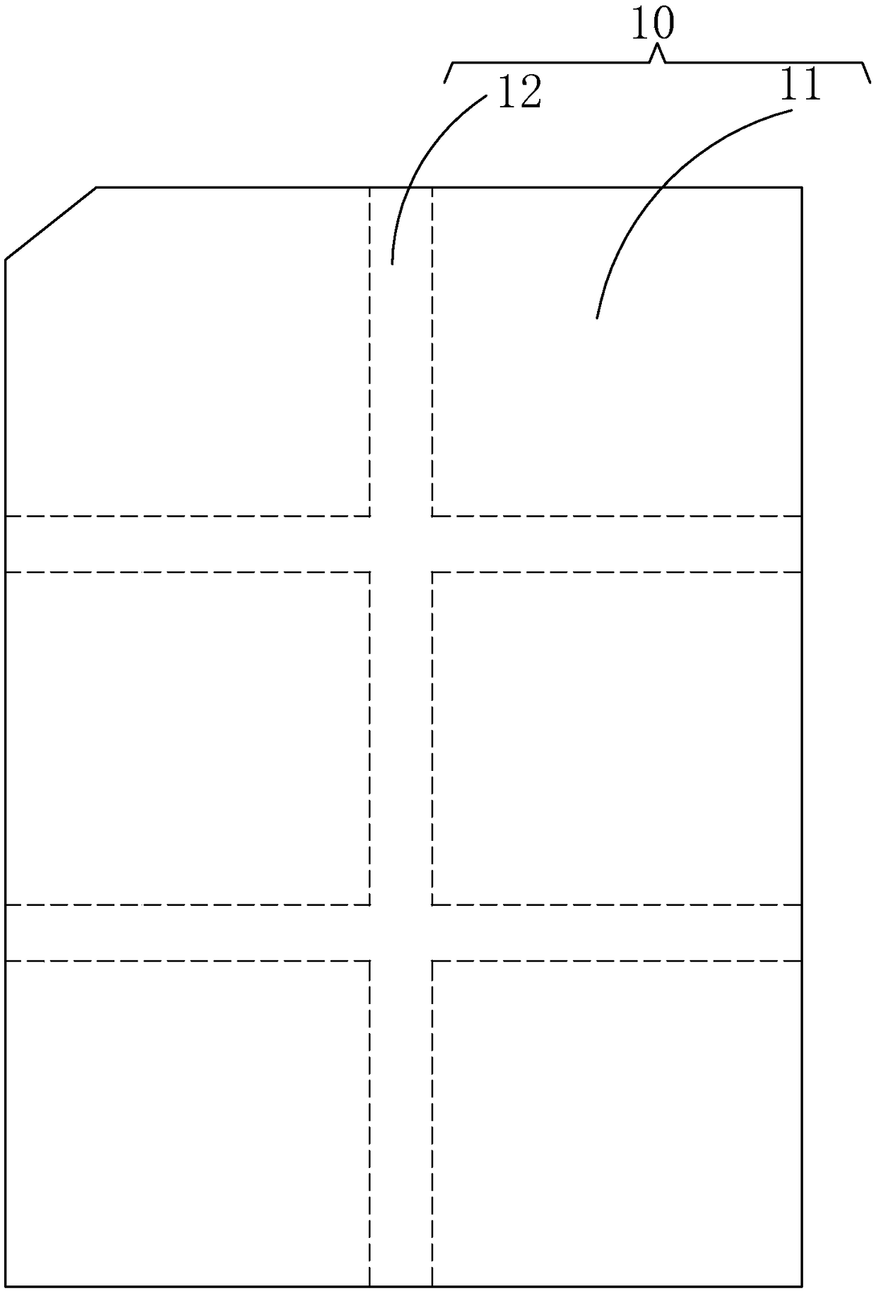
[0031] Step S1, please refer to figure 2 , A motherboard 10 is provided. The motherboard 10 includes a plurality of panel regions 11 arranged in an array and a spacer region 12 located between each adjacent panel region 11.
[0032] Such as figure 1 As shown, in a preferred embodiment of the present invention, the mother board 10 is a glass mother board with a size of 730mm×920mm. The mother board 10 includes 6 panel areas 11 arranged in an array, and the spacer area 12 is located Between each adjacent panel area 11, the panel area 11 is used to form various elements required in the display panel, such as ...
PUM
| Property | Measurement | Unit |
|---|---|---|
| width | aaaaa | aaaaa |
| thickness | aaaaa | aaaaa |
| angle | aaaaa | aaaaa |
Abstract
Description
Claims
Application Information
 - R&D
- Intellectual Property
- Life Sciences
- Materials
- Tech Scout
- Unparalleled Data Quality
- Higher Quality Content
- 60% Fewer Hallucinations
Browse by: Latest US Patents, China's latest patents, Technical Efficacy Thesaurus, Application Domain, Technology Topic, Popular Technical Reports.
© 2025 PatSnap. All rights reserved.Legal|Privacy policy|Modern Slavery Act Transparency Statement|Sitemap|About US| Contact US: help@patsnap.com