

Image processing based cable semi-conductive layer automatic detection method
A semi-conductive layer and image processing technology, applied in image data processing, image enhancement, image analysis, etc., can solve problems such as many calculation items, calculation errors, and complicated manual measurement
- Summary
- Abstract
- Description
- Claims
- Application Information
AI Technical Summary
Problems solved by technology
Method used
Image

Examples
Embodiment Construction
[0069] In order to describe the present invention more specifically, the technical solutions of the present invention will be described in detail below in conjunction with the accompanying drawings and specific embodiments.
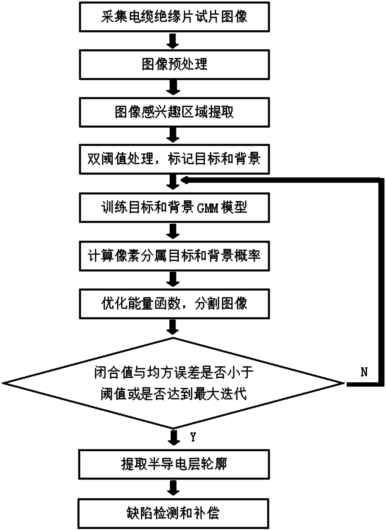
[0070] Such as figure 1 As shown, an image processing-based automatic detection method for the semiconducting layer of an insulating sheet includes the following steps:
[0071] (1) Select a test piece of the cable to be tested with less knife marks and a relatively obvious boundary between the semiconductive layer and the insulating layer, use the cover glass to flatten the test piece to eliminate the interference of the test piece from warping and bending, and then adjust the light source to Appropriate location and light intensity;
[0072] (2) Use a high-resolution industrial camera to collect test piece images;
[0073] (3) Perform image preprocessing on the collected test piece image: gray scale, threshold value:
[0074] Image grayscale:
[007...
PUM
 Abstract
Description
Claims
Application Information