Circuit repairing method for printed circuit board

A printed circuit board and circuit board technology, applied in the directions of printed circuit maintenance/correction, printed circuit secondary processing, etc., can solve the problems of high production cost and low printed circuit board yield, so as to improve production yield and reduce production. cost effect

Active Publication Date: 2018-11-20
SHENZHEN BAROY NEW MATERIAL TECH CO LTD
View PDF5 Cites 13 Cited by
  • Summary
  • Abstract
  • Description
  • Claims
  • Application Information

AI Technical Summary

Problems solved by technology

[0003] The purpose of the present invention is to provide a circuit repair method for printed circuit boards to solve the technical problems of low yi

Method used


Image

  • Circuit repairing method for printed circuit board
  • Circuit repairing method for printed circuit board
  • Circuit repairing method for printed circuit board

Examples


specific Embodiment approach

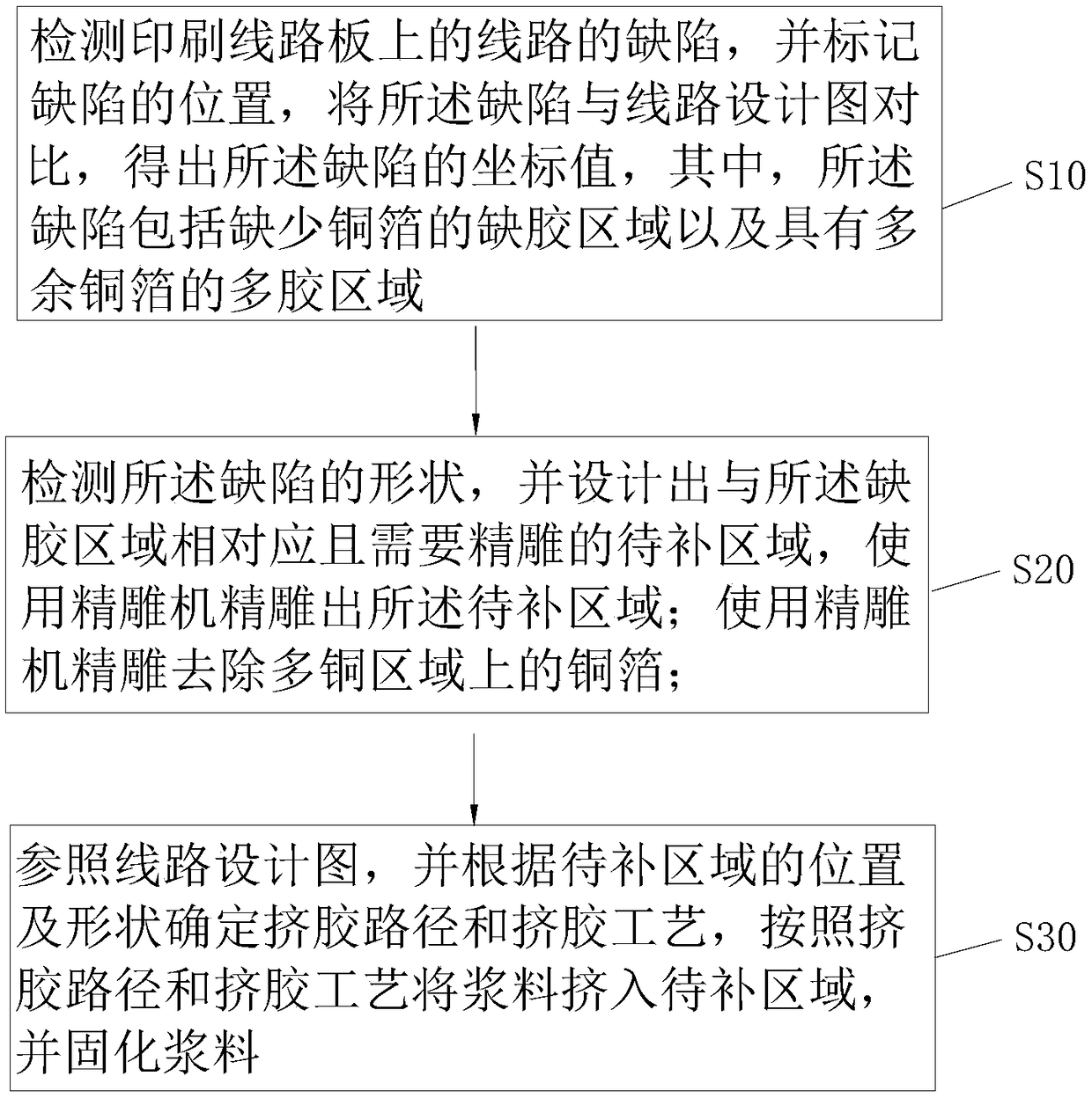
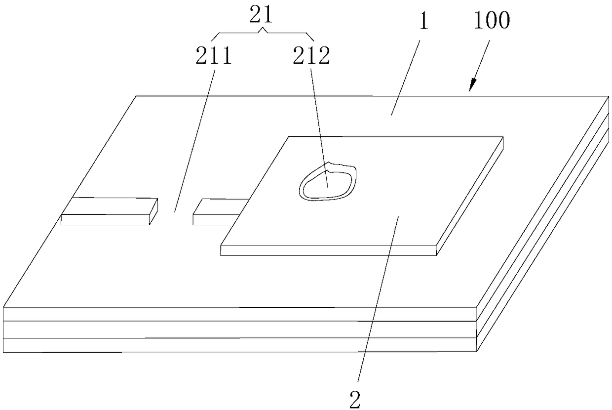
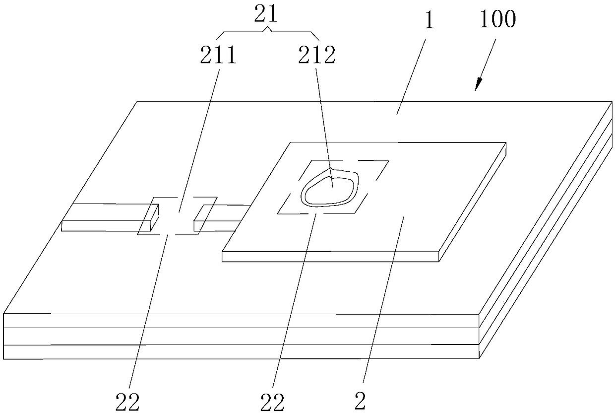
[0046] Further, as a specific embodiment of the circuit repair method for printed circuit boards provided by the present invention, detecting the shape of the defect includes the following steps:

[0047] Using full laser scanning, step probe scanning or optical 3D scanning on the surface of the circuit board 100 to detect height changes on the surface of the circuit board 100 and draw a first digital model of the surface height changes;

[0048] Taking the smooth height change in the first digital model as the warpage of the plate, and converting the first digital model into the second digital model through warpage correction;

[0049] Comparing the second digital model with the circuit design diagram, the region with a positive height difference greater than a predetermined value is in the shape of a copper-rich region, and the region with a negative height difference greater than a predetermined value is in the shape of a copper-deficient region 21 .

[0050] Wherein, the s...


PUM


Abstract

The invention provides a circuit repairing method used for a printed circuit board, comprising the following steps: firstly detecting a circuit on the printed circuit board, marking a position of a defect on the circuit, comparing the defect with a circuit design drawing, and obtaining coordinate values of the defect; then detecting a shape of the defect, designing and carving a to-be-repaired region according to the shape of the defect, and carving and removing a copper foil in a copper-rich region by using a carving machine; and finally referring to the circuit design drawing, determining aglue extrusion path and a glue extrusion technology according to the position and shape of the to-be-repaired region, extruding slurry into the to-be-repaired region according to the glue extrusion path and the glue extrusion technology, and solidifying the slurry. The provided circuit repairing method used for the printed circuit board has the advantages that the position and shape of the defectare detected, the copper-rich region and a copper-deficient region are carved, a short circuit defect is eliminated, then the to-be-repaired region is filled by using the slurry, repairing on the defects such as circuit breakage and a pit is realized, and production yield of the printed circuit board is improved.

Description

technical field [0001] The invention belongs to the technical field of manufacturing printed circuit boards, and more specifically relates to a circuit repair method for printed circuit boards. Background technique [0002] A printed circuit board is a circuit substrate with printed wiring, which is used to mount and connect circuit components. In the manufacturing process of printed circuit boards, due to the high resolution of the conductive lines and the difficulty of the process, various manufacturing defects will appear in the process of making conductive lines. Most of the defects of conductive lines are line damage, Dimples, air holes, short circuits, etc. In this way, the production yield of the printed circuit board is low, which indirectly increases the production cost. Contents of the invention [0003] The purpose of the present invention is to provide a circuit repair method for printed circuit boards, so as to solve the technical problems in the prior art t...

Claims


Application Information

Patent Timeline
IPC IPC(8): H05K3/22
CPCH05K3/225
Inventor 郭冉胡军辉齐学亮
Owner SHENZHEN BAROY NEW MATERIAL TECH CO LTD
Why Eureka
Try Eureka