
Semiconductor power device and manufacturing method thereof

A technology of power devices and semiconductors, applied in the direction of semiconductor devices, electrical components, circuits, etc., can solve problems such as occupying a large space, affecting packaging by chips, integration and volume of modules, and high production costs, so as to increase stability and solve problems The effect of photolithography process on bias and reducing production cost

Active Publication Date: 2022-05-20
BYD SEMICON CO LTD
View PDF4 Cites 0 Cited by
  • Summary
  • Abstract
  • Description
  • Claims
  • Application Information

AI Technical Summary

Problems solved by technology

However, this will make it difficult to reduce the size of the device, especially for high-current devices. In order to realize that the device can work in a high-current state, it is necessary to connect a large number of cells in parallel to form a large device, so that the current density of the cells Directly determine the size of the final chip, so the chip area will be relatively large, and the production cost will be relatively high
In addition, the size of the chip will also affect the integration and volume of the subsequent packaging and modules. The large volume will occupy a large space in the application, which is not conducive to the high integration of the product
[0004] Therefore, the manufacturing method of semiconductor power devices at this stage still needs to be improved.

Method used


Image

  • Semiconductor power device and manufacturing method thereof
  • Semiconductor power device and manufacturing method thereof
  • Semiconductor power device and manufacturing method thereof

Examples


Embodiment Construction

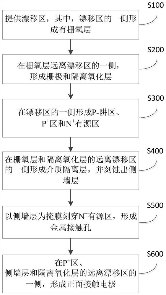
[0050] The following describes the embodiments of the present invention in detail, and those skilled in the art will understand that the following embodiments are intended to explain the present invention, and should not be regarded as limiting the present invention. Unless otherwise specified, in the following examples that do not explicitly describe specific techniques or conditions, those skilled in the art can carry out according to commonly used techniques or conditions in this field or according to product instructions. The reagents or instruments used were not indicated by the manufacturer, and they were all commercially available conventional products.

[0051] In one aspect of the invention, the invention proposes a semiconductor power device. refer to figure 1 , to describe the semiconductor power device of the present invention in detail.

[0052] According to an embodiment of the present invention, refer to figure 1 , the semiconductor power device includes: a d...


PUM


Abstract

The present invention proposes a semiconductor power device and a manufacturing method thereof. The semiconductor power device includes: a drift region; a P-well region, which is arranged on one side of the drift region; P + region, set on the side of the P-well region away from the drift region; N + active area, set at P + The side of the gate oxide layer away from the drift region; the gate oxide layer is arranged on the side of the P-well region away from the drift region; the gate is arranged on the side of the gate oxide layer away from the drift region; the isolation oxide layer is arranged on the gate away from the drift region One side of the zone; side wall layer, set at N + The active region is away from the side of the drift region, and is in direct contact with the gate oxide layer, the sidewall of the gate and the isolation oxide layer; and the front contact electrode is arranged on the P + The side of the drift region, the sidewall layer and the isolation oxide layer away from the drift region. In the semiconductor power device proposed by the present invention, the newly added sidewall layer can solve the alignment problem of the photolithography process, and at the same time reduce the width, so that the stability is better, the power device area is smaller, and the integration degree is higher. And the production cost is lower.

Description

technical field [0001] The present invention relates to the technical field of semiconductors, and in particular, the present invention relates to semiconductor power devices and manufacturing methods thereof. Background technique [0002] At present, in the manufacturing process of MOS type semiconductor power devices, each layer except the P-well region (P-Well region) is basically aligned and etched through the photolithography process, but the photolithography process has unavoidable impact. Offset problem, which will reduce the stability of the manufactured MOS semiconductor power devices. [0003] At this stage, in order to solve the problem of alignment technology in the lithography process, it is necessary to reserve enough space for each layer structure to ensure that the device will not fail due to the alignment of lithography. However, this will make it difficult to reduce the size of the device, especially for high-current devices. In order to realize that the d...

Claims


Application Information

Patent Timeline
Patent Type & Authority Patents(China)
IPC IPC(8): H01L29/423H01L21/28
CPCH01L29/401H01L29/42364
Inventor 朱辉肖秀光吴海平
Owner BYD SEMICON CO LTD
Features
  • Generate Ideas
  • Intellectual Property
  • Life Sciences
  • Materials
  • Tech Scout
  • Unparalleled Data Quality
  • Higher Quality Content
  • 60% Fewer Hallucinations
Learn More