Display plasma module of dual-layer microstructure and manufacturing method of display plasma module

A microstructure and plasma technology, which is used in the manufacture of electrode systems, the manufacture of discharge tubes/lamps, and the manufacture of cold cathodes, to achieve the effects of improving contrast and display effect, good display effect and reducing manufacturing cost.

Active Publication Date: 2018-12-07
WUXI VISION PEAK TECH
View PDF8 Cites 2 Cited by
  • Summary
  • Abstract
  • Description
  • Claims
  • Application Information

AI Technical Summary

Problems solved by technology

[0008] The purpose of the present invention is to provide a display plasma module with a double-layer microstructure and its manufacturing method for the problems of the current electronic display screen, which can directly use the display plasma to replace the existing microcup structure or microcapsule, and The display plasma is equipped with a plasma barrier array and a spacer particle layer for uniformly dispersing, stabilizing and isolating the display plasma, which plays the role of supporting the electrodes and controlling the thickness of the display plasma, while effectively preventing the disordered flow of the display plasma. The verticality of the electric field direction between the pixel electrode and the transparent electrode is guaranteed

Method used


Image

  • Display plasma module of dual-layer microstructure and manufacturing method of display plasma module
  • Display plasma module of dual-layer microstructure and manufacturing method of display plasma module

Examples


Embodiment Construction

[0040] The present invention will be further described below in conjunction with specific drawings and embodiments.

[0041] The present invention is not limited to the following embodiments, and the figures referred to in the following description are provided for understanding the content of the present invention, that is, the present invention is not limited to the structure of the electronic ink display screen exemplified in each figure.

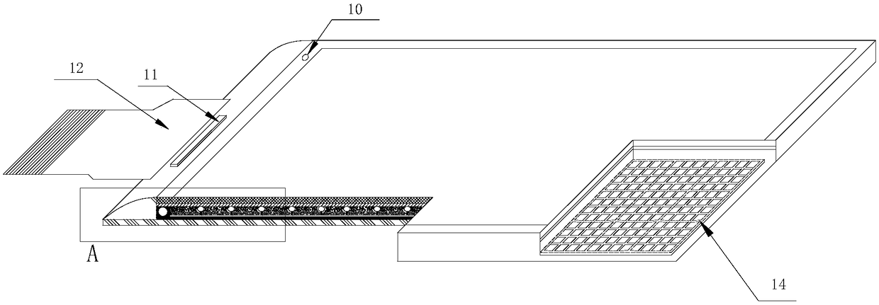
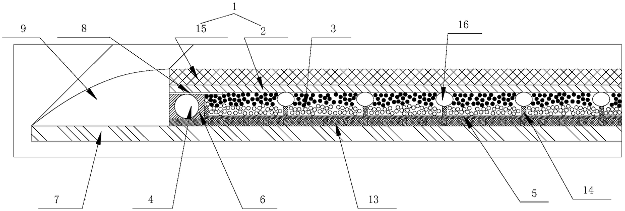
[0042] as attached figure 1 with figure 2 As shown, Embodiment 1 takes a dual-particle electronic ink display screen as an example, a display plasma module with a double-layer microstructure, including a pixel electrode 13 and a transparent electrode 1 located above the pixel electrode 13, the pixel electrode 13 and A display plasma 3 and a liner frame 6 surrounding the display plasma 3 are arranged between the transparent electrodes 1, and a plasma barrier array 14 for uniformly dispersing and stabilizing the display plasma 3 is arran...


PUM

PropertyMeasurementUnit
widthaaaaaaaaaa
heightaaaaaaaaaa
thicknessaaaaaaaaaa

Abstract

The invention belongs to the technical field of electronic display, and relates to a display plasma module of a dual-layer microstructure. The display plasma module comprises a pixel electrode and a transparent electrode located above the pixel electrode; display plasma and a lining frame surrounding the display plasma are arranged between the pixel electrode and the transparent electrode, plasmastopping and isolating arrays for uniformly dispersing and stabilizing the display plasma are arranged on the pixel electrode and / or the transparent electrode, and spaced particle layers are adsorbedon the plasma stopping and isolating arrays. The display plasma is directly adopted for the display plasma arrays to replace existing microcup structures or microcapsules, the plasma stopping and isolating arrays for uniformly dispersing, stabilizing and isolating the display plasma and the spaced particle layers are arranged in the display plasma, and the effects of supporting the whole display plasma module and controlling the thickness of the display plasma are achieved; meanwhile, disordered flow of the display plasma is effectively prevented, and the perpendicularity of the direction of an electric field between the pixel electrode and the transparent electrode is guaranteed.

Description

technical field [0001] The invention relates to a display plasma module and a manufacturing method thereof, in particular to a display plasma module with a double-layer microstructure and a manufacturing method thereof, belonging to the technical field of electronic display. Background technique [0002] Electrophoretic display utilizes the phenomenon of swimming of charged colloidal particles under the action of an electric field, and drives electrophoretic particles with different photoelectric properties through the electric field to realize the display of images and text. Compared with known display technologies, electrophoretic display has the following characteristics: flexible It is easy to bend, light in weight, thin in thickness, high in contrast, low in energy consumption, wide in viewing angle, readable in sunlight, has image bistable state, and is easy to produce on a large scale. [0003] Electrophoretic display technology was first proposed in the 1970s. Paten...

Claims


Application Information

Patent Timeline
Patent Type & Authority Applications(China)
IPC IPC(8): G02F1/167G02F1/1339G02F1/1343G02F1/1335G02F1/1333
CPCG02F1/1333G02F1/133512G02F1/13394G02F1/134309G02F1/167H01J11/22H01J11/34H01J11/46H01J9/261G02F1/16757G02F1/1681G02F1/16756G02F1/1679G02F1/1676G02F2201/50
Inventor 张磊包进陈山
Owner WUXI VISION PEAK TECH
Why Eureka
Try Eureka