Chip alignment mounting device and method

A mounting device and chip mounting technology, which is applied in the direction of electrical components, semiconductor/solid-state device manufacturing, circuits, etc., can solve problems such as unfavorable, increasing the total time of chip mounting, shortening the time of mounting chips, etc., to improve production efficiency Effect

Active Publication Date: 2018-12-07
TANGREN MICROTELLIGENCE TECH CO LTD
View PDF6 Cites 6 Cited by
  • Summary
  • Abstract
  • Description
  • Claims
  • Application Information

AI Technical Summary

Problems solved by technology

[0005] One of the defects of this type of chip mounting device and method is that the chip bonding mechanism performs translational motion. In the process of returning to the chip supply mechanism from the chip position and the chip placement work area, at least two acceleration movements and two deceleration movements are required. Frequent position movement and speed addition and subtraction are not conducive to shortening the chip placement time and controlling the chip placement the accuracy of
In addition, the second defect of this type of chip mounting device and method is that in a chip mounting cycle, the chip bonding mechanism picks up the chip from the chip supply mechanism, the chip bonding mechanism transports the chip to the predetermined placement position, and the visual imaging The process of imaging and aligning the chip by the mechanism, and mounting the chip on the predetermined placement position by the chip bonding mechanism are all carried out serially, that is, the next process can only be carried out after completing the previous process, which makes the process sequence of chip mounting Single and fixed, further increasing the total time required for die attach
[0006] Therefore, in order to simultaneously improve the placement accuracy and production efficiency of semiconductor chips on the substrate, it is urgent to propose a new chip alignment and placement device and its method, so as to solve the problem that existing equipment and methods cannot quickly complete the alignment of chips and substrates. Technical issues of standard and mounting

Method used


Image

  • Chip alignment mounting device and method
  • Chip alignment mounting device and method
  • Chip alignment mounting device and method

Examples


Embodiment Construction

[0056] In order to make the purpose, technical solutions and advantages of the embodiments of the present invention clearer, the technical solutions in the embodiments of the present invention will be clearly and completely described below in conjunction with the drawings in the embodiments of the present invention. Obviously, the described embodiments It is only some embodiments of the present invention, but not all embodiments. Based on the embodiments of the present invention, all other embodiments obtained by persons of ordinary skill in the art without making creative efforts belong to the protection scope of the present invention.

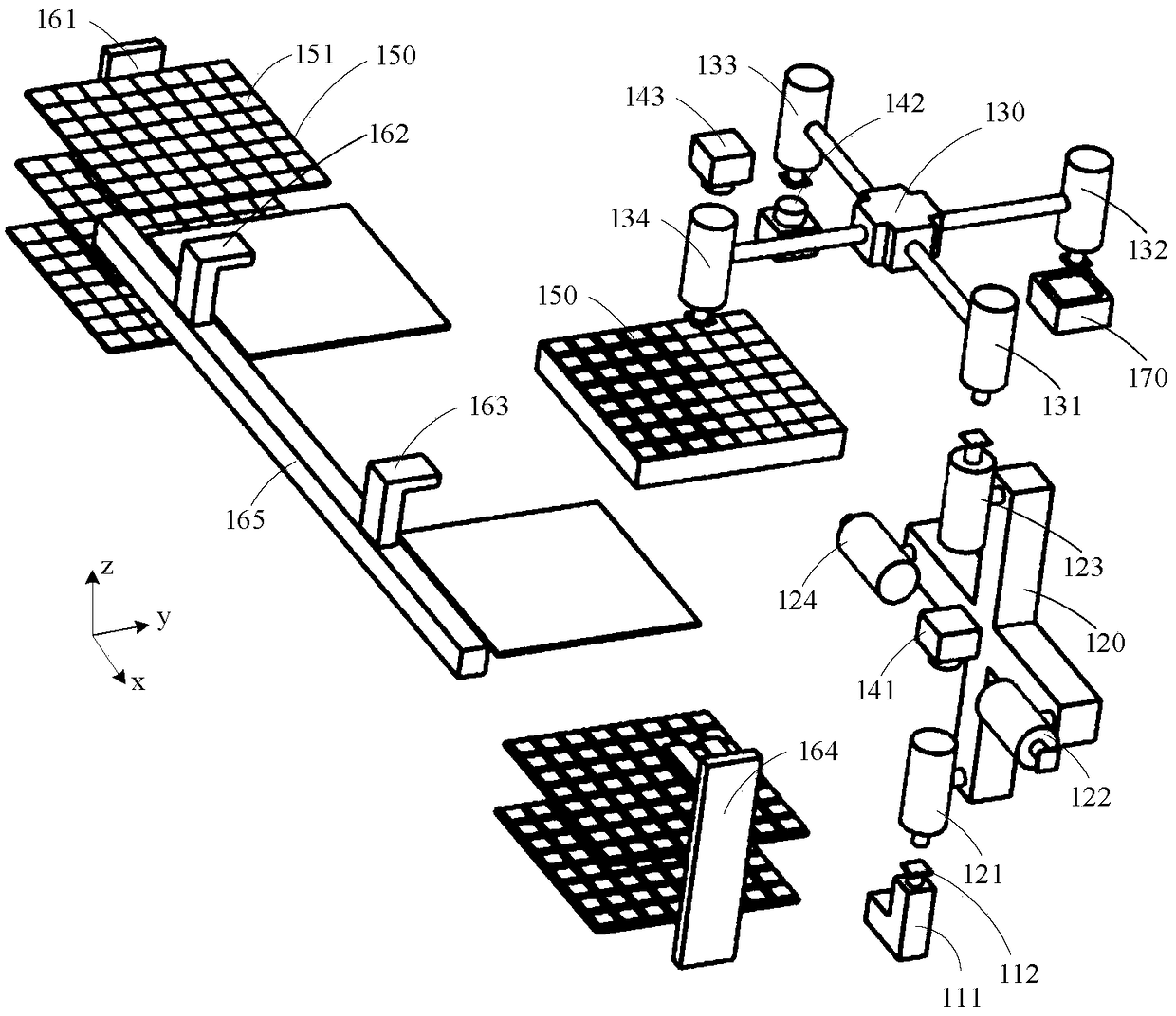
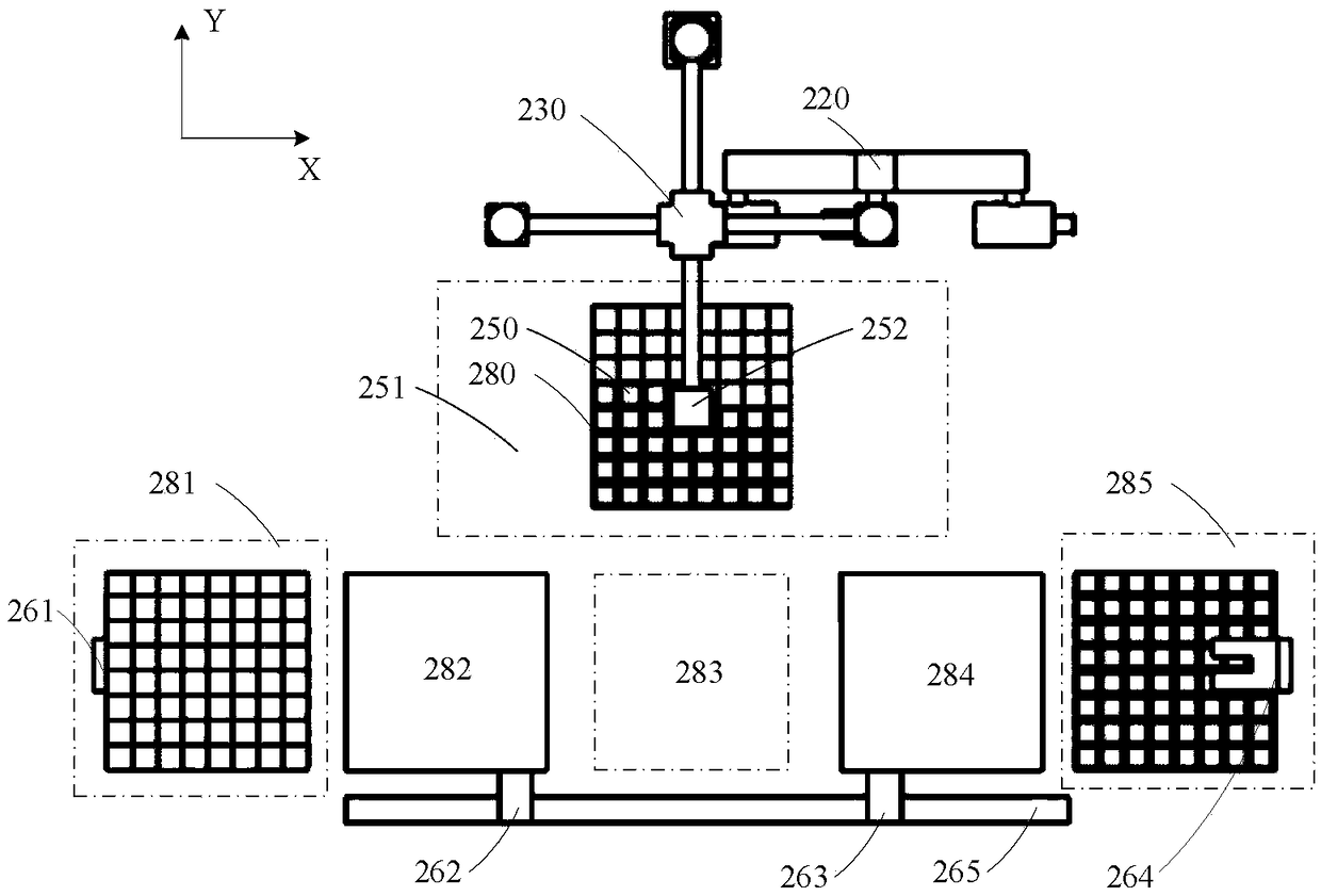
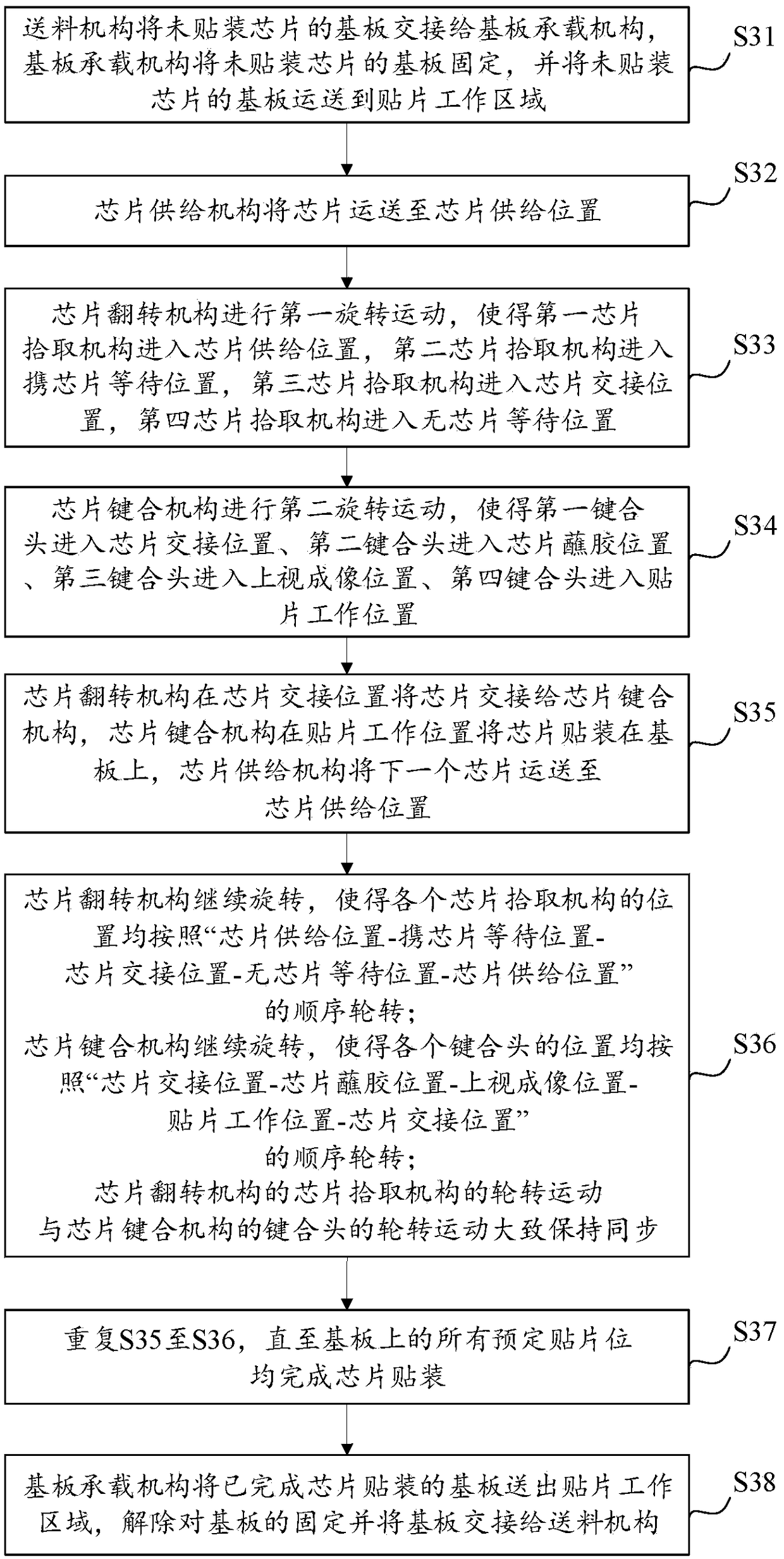
[0057] An embodiment of the present invention provides a chip alignment and placement device. The chip alignment and placement device provided by the present invention includes a substrate carrying mechanism, a chip supply mechanism, a chip turning mechanism, a chip bonding mechanism, an alignment and imaging mechanism, and a material feeding...


PUM


Abstract

The present invention provides a chip alignment mounting device. The chip alignment mounting device comprises a feed mechanism, a substrate carrying mechanism, a chip supply mechanism, a chip turnovermechanism and a chip bonding mechanism, the feed mechanism is configured to provide a substrate without mounting a chip and remove a substrate with a mounted chip; the substrate carrying mechanism isconfigured to load and fix the substrate and drive the substrate to move on a first plane; the chip supply mechanism is configured to provide the chip at the chip supply position on the chip supply mechanism; the chip supply mechanism can pick up the chip from the chip supply position, transmit the chip to a chip handover position through rotation motion and supply the chip to the chip bonding mechanism; the chip bonding mechanism is configured to pick up the chip from the chip handover position and mount the chip to a pre-determined mounting position through rotation motion; and the mountingoperation position, the chip supply position and the chip handover position are fixed positions. The present invention further provides a chip alignment mounting method. The chip mounting efficiencyand precision can be improved.

Description

technical field [0001] The invention relates to the technical field of semiconductor device packaging, in particular to a chip alignment and placement device and method thereof. Background technique [0002] With the continuous development of modern information technology and consumer electronics products, integrated circuit chips are increasingly developing in the direction of high density, high performance, light weight and short size. Chips manufactured using traditional packaging and interconnection technologies such as TO, DIP, PLCC, and QFP have been difficult to meet the increasing performance requirements of chips. Therefore, semiconductor packaging and assembly technologies such as flip-chip, fan-out packaging, and three-dimensional packaging Integrated advanced packaging technology emerged as the times require to reduce device package size, increase interconnection density, improve integrated circuit chip performance, and reduce product prices. [0003] The existi...

Claims


Application Information

Patent Timeline
Patent Type & Authority Applications(China)
IPC IPC(8): H01L21/67
CPCH01L21/67092H01L21/67144H01L21/67259
Inventor 唐亮丁晨阳成冰峰郝术壮
Owner TANGREN MICROTELLIGENCE TECH CO LTD
Why Eureka
Try Eureka