Packaging structure and manufacturing method of a thick-film hybrid integrated circuit

A packaging structure, integrated circuit technology, applied in the direction of circuits, electrical components, electrical solid devices, etc., can solve the problems of low assembly density, inconvenient miniaturization design of electronic components, etc.

Active Publication Date: 2020-10-16
BEIJING SUPLET
View PDF3 Cites 4 Cited by
  • Summary
  • Abstract
  • Description
  • Claims
  • Application Information

AI Technical Summary

Problems solved by technology

[0003] The assembly density of components in the packaging structure of the prior art thick-film hybrid integrated circuit is low, resulting in the need for a large-area thick-film film-forming substrate, which is not convenient for the miniaturization design of electronic components

Method used


Image

  • Packaging structure and manufacturing method of a thick-film hybrid integrated circuit
  • Packaging structure and manufacturing method of a thick-film hybrid integrated circuit
  • Packaging structure and manufacturing method of a thick-film hybrid integrated circuit

Examples


Embodiment Construction

[0045] The following will clearly and completely describe the technical solutions in the embodiments of the present invention with reference to the accompanying drawings in the embodiments of the present invention. Obviously, the described embodiments are only some, not all, embodiments of the present invention. Based on the embodiments of the present invention, all other embodiments obtained by persons of ordinary skill in the art without making creative efforts belong to the protection scope of the present invention.

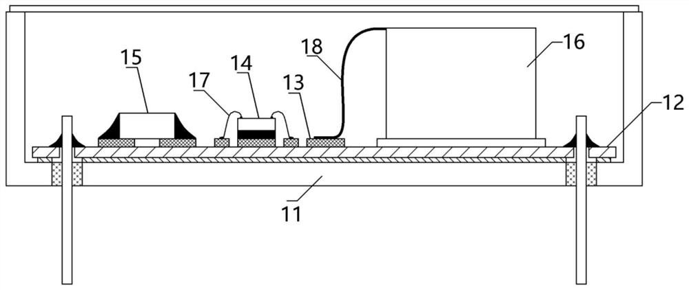
[0046] Such as figure 1 As shown, the existing thick-film hybrid integrated circuit is a typical single-layer assembly structure, and components (including chips 14, chip components 15, magnetic inductors and transformers 16, etc.) assembly, due to the large difference in the assembled height of each component: for example, the assembled height of the chip 14 is between 0.6mm and 1.0mm, and the assembled height of the chip component 15 is between 0.5mm and 2.5...


PUM


Abstract

The invention discloses a package structure of a thick film hybrid integrated circuit and a manufacturing method of the package structure. According to the package structure of the thick film hybrid integrated circuit provided by the technical schemes of the present invention, a support structure is mounted on a thick film formation substrate, so that a first type of components can be assembled through the thick film formation substrate and the support structure, and therefore, a 3D package structure can be formed, the assembly area of the first type of components in a product can be increased, the assembly density of the thick film hybrid integrated circuit product can be increased, and the miniaturization design of an electronic device can be facilitated.

Description

technical field [0001] The present invention relates to the technical field of packaging of hybrid integrated circuits, more particularly to a packaging structure of thick-film hybrid integrated circuits and a manufacturing method thereof. Background technique [0002] The thick-film hybrid integrated circuit is an airtight package device, and the interior is sealed with high-purity nitrogen to ensure that the fragile components such as bare chips and bonding wires in the product are completely isolated from the external unfavorable environment. Its products have a wide operating temperature range and good environmental adaptability. , high reliability, widely used in fields with high reliability requirements. refer to figure 1 , figure 1 It is a schematic diagram of the packaging structure of the prior art thick film hybrid integrated circuit, figure 1 The packaging structure shown adopts an all-metal airtight packaging casing 11; a thick film film-forming substrate 12 i...

Claims


Application Information

Patent Timeline
Patent Type & Authority Patents(China)
IPC IPC(8): H01L23/31H01L23/488H01L21/60
CPCH01L23/3114H01L23/3121H01L23/488H01L24/03H01L2224/32225H01L2224/48091H01L2224/48227H01L2224/73265H01L2924/15159H01L2924/19105H01L2924/19106H01L2924/00014H01L2924/00
Inventor 许艳军刘笑嫘吴斌
Owner BEIJING SUPLET
Why Eureka
Try Eureka