

A 3D stacked structure of an ltcc substrate
A stacked structure and substrate technology, applied in the field of microelectronics, can solve the problems of low mechanical strength, high welding difficulty, low assembly area ratio, etc., and achieve the effect of increasing mechanical strength, improving assembly efficiency, and alleviating assembly difficulty
- Summary
- Abstract
- Description
- Claims
- Application Information
AI Technical Summary
Problems solved by technology
Method used
Image

Examples
Embodiment Construction
[0024] The present invention will be described in detail below in conjunction with the accompanying drawings.
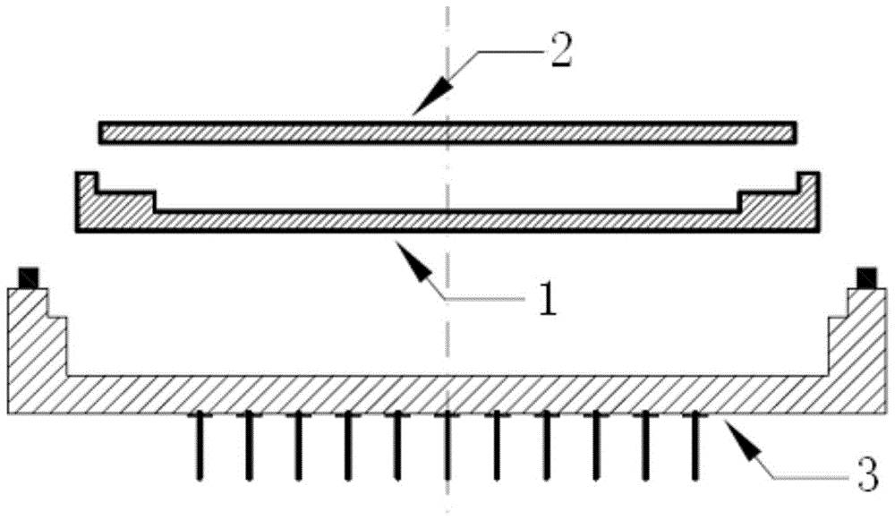
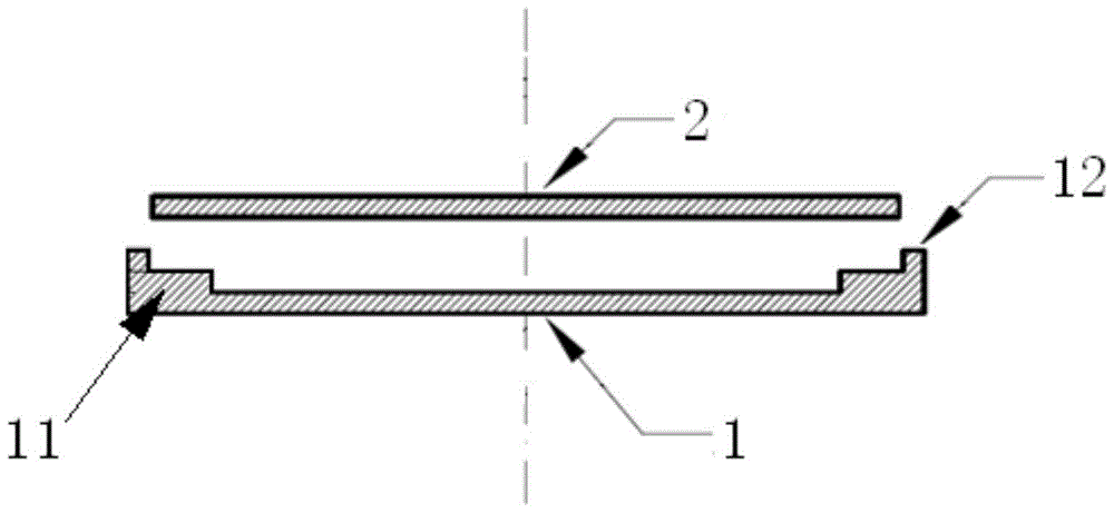
[0025] Such as figure 1 , 2 As shown, the present invention provides a 3D stacked structure of LTCC substrates, including: several stacked LTCC substrate structures, the LTCC substrate structures are connected by I / O interconnection and mechanical connection; several stacked LTCC substrate structures A housing 3 for encapsulation is provided on the outside; wherein, the LTCC substrate structure includes a lower substrate 1 and an upper substrate 2, the upper substrate 2 is fastened on the lower substrate 1, a cavity is formed between the lower substrate 1 and the upper substrate 2, and the lower substrate 1 Both the upper substrate 2 and the upper substrate 2 can be arranged with components. Specifically, the edge of the lower substrate 1 is sequentially provided with a first step 11 for mechanically fixing the upper substrate 2 and the lower substrate 1 and a seco...
PUM
 Abstract
Description
Claims
Application Information