Electronic device and manufacturing method thereof

A technology of electronic devices and manufacturing methods, which is applied in the direction of final product manufacturing, sustainable manufacturing/processing, semiconductor/solid-state device manufacturing, etc., and can solve problems such as high equipment cost, limited density of electronic device components, and limited equipment manufacturing accuracy. Achieve the effect of increasing the density of component settings

Active Publication Date: 2018-12-07
PANELSEMI CORP
View PDF9 Cites 3 Cited by
  • Summary
  • Abstract
  • Description
  • Claims
  • Application Information

AI Technical Summary

Problems solved by technology

However, the cost of equipment required by this manufacturing method is relatively high, which makes the cost of the electronic device relatively high, and is limited by the manufacturing accuracy of the equipment, so that the component density of the manufactured electronic device is also limited

Method used


Image

  • Electronic device and manufacturing method thereof
  • Electronic device and manufacturing method thereof
  • Electronic device and manufacturing method thereof

Examples


Embodiment Construction

[0027] The electronic device and its manufacturing method according to preferred embodiments of the present invention will be described below with reference to related drawings, wherein the same elements will be described with the same reference numerals.

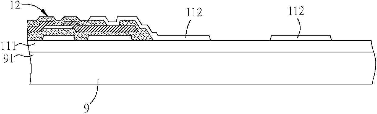
[0028] Please refer to figure 1 , which is a schematic flowchart of a method for manufacturing an electronic device according to a preferred embodiment of the present invention. The electronic device described in the following embodiments can be a light-emitting diode (LED) display, a micro-light-emitting diode display (Micro-LED Display), a sensing device (such as a fingerprint sensor, a fingerprint reader, an X-ray sensor), a semiconductor devices or lighting devices, etc., the present invention does not make any limitation here.

[0029] Such as figure 1 As shown, the manufacturing method of the electronic device 1 includes the following steps: forming a flexible substrate (Flexible Substrate) on a rigid carrier (step ...


PUM


Abstract

The invention provides an electronic device and a manufacturing method thereof. The invention discloses the electronic device and the manufacturing method thereof. The manufacturing method of the electronic device comprises the following steps: forming a flexible substrate on a rigid carrier plate; forming at least one thin film element on the flexible substrate; forming a conductive line on the flexible substrate, wherein the conductive line is electrically connected with the thin film element, and the line width of the conductive line is between 1 and 10 microns; forming at least one electrical connection pad on the flexible substrate, wherein the electrical connection pad is electrically connected with the conductive line, and the thickness of the electrical connection pad is between 2and 20 microns; arranging at least one surface mount device on the flexible substrate, wherein the surface mount device is electrically connected with the thin film element through the electrical connection pad and the conductive line; and removing the rigid carrier plate.

Description

technical field [0001] The present invention relates to an electronic device, in particular, to an electronic device and a manufacturing method thereof. Background technique [0002] Traditionally, in the process of manufacturing electronic devices (such as displays), the semiconductor elements are obtained one by one by semiconductor technology and then transposed on the carrier substrate, and then use the pick-up head to self-support the substrate After capturing one or more components last time, they can be transposed onto, for example, a circuit substrate, and then other subsequent processes are performed. However, the cost of equipment required by this manufacturing method is relatively high, which makes the cost of the electronic device relatively high, and is limited by the manufacturing accuracy of the equipment, so that the component density of the electronic device is also limited. Contents of the invention [0003] The purpose of the present invention is to pro...

Claims


Application Information

Patent Timeline
Patent Type & Authority Applications(China)
IPC IPC(8): H01L27/12H01L27/15H01L21/683
CPCH01L21/6835H01L27/1214H01L27/1259H01L27/156H01L2221/68386Y02E10/549Y02P70/50H10K39/32H10K59/131H10K77/111H10K71/80H10K59/1201H10K2102/351H10K2102/311H05K1/189H05K1/16H05K3/3436H05K2201/10128H01L25/0753H01L33/62H01L25/167H01L2933/0066H01L33/486H01L2933/0033H01L21/32133H01L24/16H01L24/81H01L27/1218H01L27/124H01L27/1266H01L27/127H01L2224/16145H01L2224/81005H01L2924/12041H01L2924/13069
Inventor 杨武璋
Owner PANELSEMI CORP
Why Eureka
Try Eureka