OLED panel and manufacturing method thereof

A manufacturing method and panel technology, applied in the field of OLED panels, can solve problems such as increasing cost, and achieve the effects of ensuring electrical connection, simplifying manufacturing process and manufacturing cost

Active Publication Date: 2018-12-07
SHENZHEN CHINA STAR OPTOELECTRONICS SEMICON DISPLAY TECH CO LTD
View PDF3 Cites 10 Cited by
  • Summary
  • Abstract
  • Description
  • Claims
  • Application Information

AI Technical Summary

Problems solved by technology

[0003] The purpose of the present invention is to provide an OLED panel and a manufacturing method thereof, so as to solve the problem in the prior art that the production of a photomask is required to increase the cost

Method used


Image

  • OLED panel and manufacturing method thereof
  • OLED panel and manufacturing method thereof
  • OLED panel and manufacturing method thereof

Examples


Embodiment Construction

[0035] The following will clearly and completely describe the technical solutions in the embodiments of the present invention with reference to the drawings in the embodiments of the present invention.

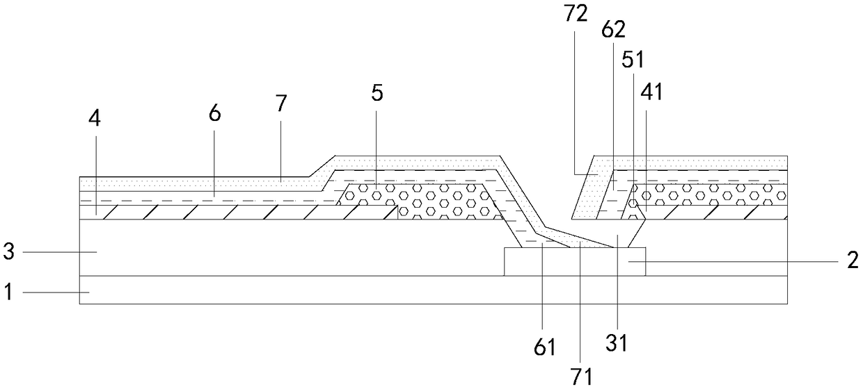
[0036] from figure 1 It can be seen that the OLED panel described in the embodiment of the present invention includes:

[0037] The substrate 1 defines that the upper part of the substrate 1 is its upper surface, and the lower part is its lower surface, wherein the substrate 1 is made of glass material.

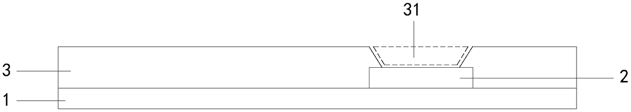
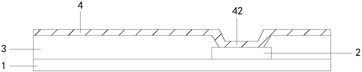
[0038] The auxiliary electrode 2 is disposed on the upper surface of the substrate 1 .

[0039] The flat layer 3, the flat layer 3 fully covers the upper surface of the substrate 1, and the flat layer 3 partially covers the auxiliary electrode 2, the space where the flat layer 3 does not cover the auxiliary electrode 2 is a hollow area 31, and the auxiliary electrode 2 is in the Appear in the hollow area 31.

[0040] The anode layer 4 is divided left and right based on the...


PUM


Abstract

The invention discloses an OLED panel and a manufacturing method thereof. The OLED panel comprises a substrate, a flat layer, an auxiliary electrode and a development layer; the flat layer is arrangedin the surface of the substrate, and provided with a hollow area; the auxiliary electrode is arranged in the hollow area; and the development is arranged in the surface of the flat layer, and comprises an electric connection part and a shielding part, the electric connection part extends into the hollow area and is electrically connected with the auxiliary electrode, the shielding part extends toa position arranged opposite to the hollow area, and the shielding part is separated from the auxiliary electrode and the electric connection part. Thus, on the premise that the hollow area is shielded and the auxiliary electrode is electrically connected, a photo mask is omitted, the manufacturing technology is simplified, the manufacturing cost is reduced, and help is provided for production ofthe OLED panel.

Description

technical field [0001] The invention relates to a technical solution in the field of OLED panels, in particular to an OLED panel and a manufacturing method thereof. Background technique [0002] In the process of OLED panel production, a part of the auxiliary electrode covered by the flat layer is hollowed out to form a hollowed out area, and then the imaging layer is electrically connected to the auxiliary electrode from both sides of the hollowed out area, because the rest of the hollowed out area will be The auxiliary electrode is exposed. In order to solve this problem, a photomask will be added in the hollow area to cover it. However, the production process of the photomask is complicated and difficult, which reduces the production efficiency and increases the production cost, which brings extremely unfavorable to the mass production of OLED influences. Contents of the invention [0003] The object of the present invention is to provide an OLED panel and a manufactur...

Claims


Application Information

Patent Timeline
Patent Type & Authority Applications(China)
IPC IPC(8): H01L27/32H01L51/52
CPCH10K59/121H10K59/00H10K50/80H10K50/84
Inventor 张良芬徐鉉植
Owner SHENZHEN CHINA STAR OPTOELECTRONICS SEMICON DISPLAY TECH CO LTD
Why Eureka
Try Eureka