Electroluminescent layer and preparation method thereof, electroluminescent device, display and illumination device
A technology of electroluminescent layer and luminescent material, which is applied in the fields of electroluminescent layer and its preparation, display and lighting devices, and electroluminescent devices, and can solve the problems of low lifespan of QLED devices
- Summary
- Abstract
- Description
- Claims
- Application Information
AI Technical Summary
Problems solved by technology
Method used
Image

Examples
preparation example Construction
[0071] The present invention provides a method for preparing an electroluminescent device in an embodiment, comprising the following steps:
[0072] Step S1: providing a substrate.
[0073] Step S2: sequentially forming the first electrode layer, the electroluminescent layer and the second electrode layer on the substrate. It can be understood that the provided substrate may have the first electrode layer, and when the first electrode layer is provided on the substrate, it is not necessary to prepare the first electrode layer.
[0074] The present invention also provides a method for preparing the above-mentioned electroluminescent layer according to an embodiment, including the method of film formation by blending and / or film formation separately.
[0075] In one embodiment, the preparation step of the film-forming method by blending includes: blending the nanocrystalline semiconductor material and the Ag complex luminescent material and forming a film to obtain an electrolu...
Embodiment 1
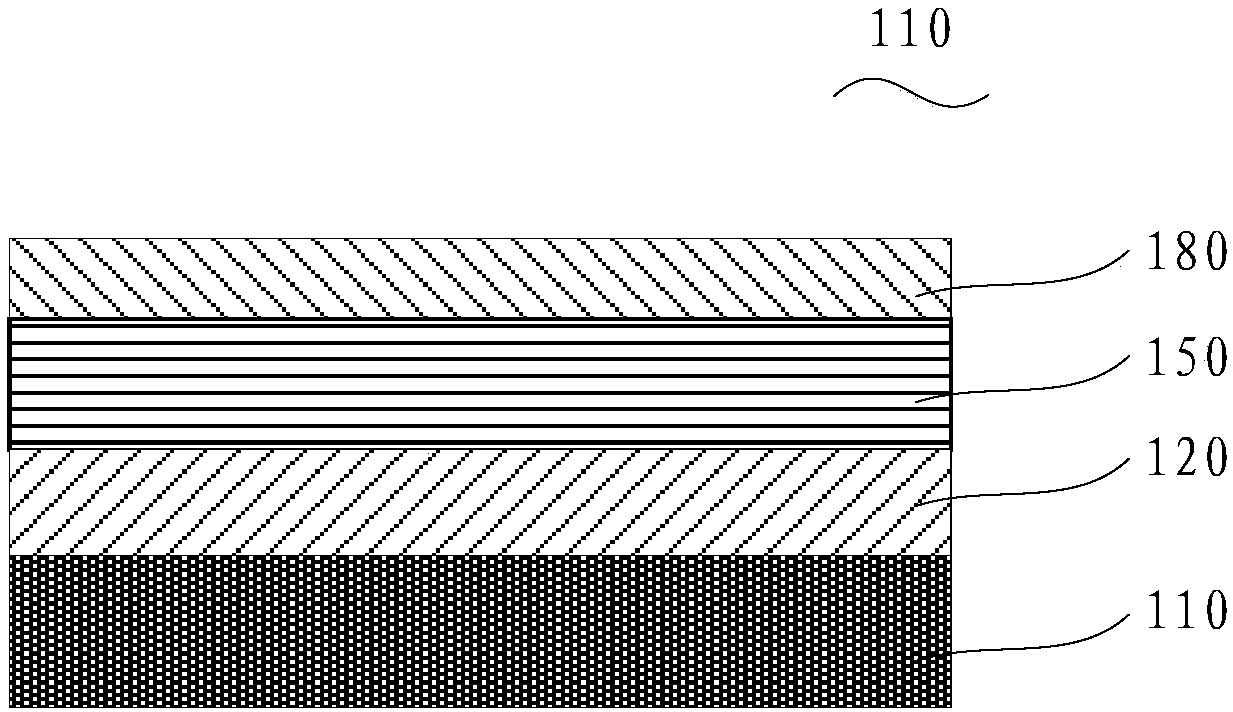
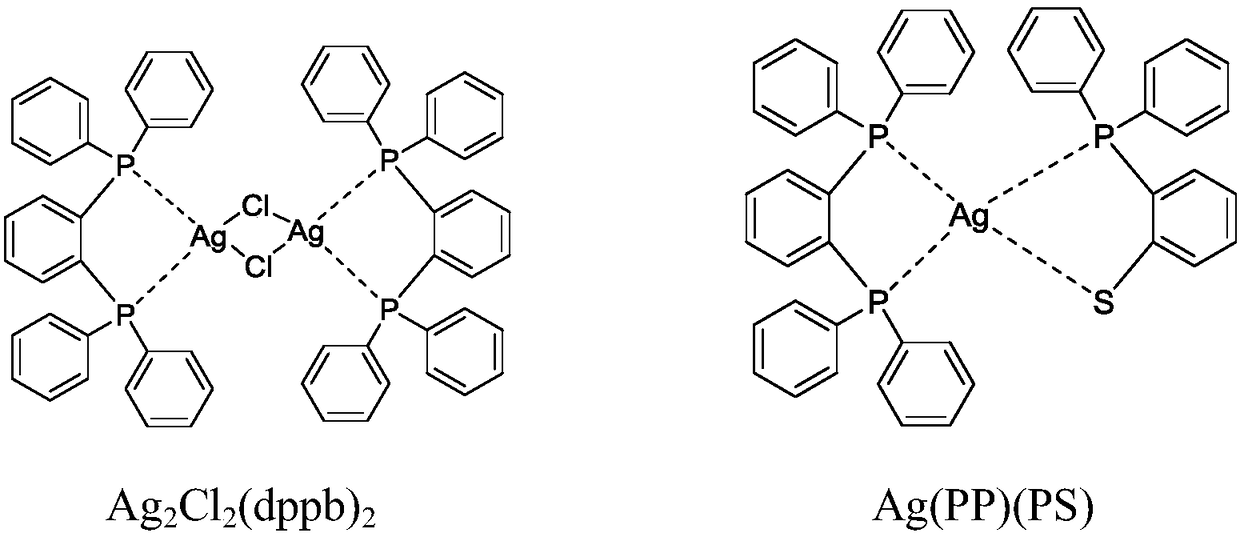
[0091] The structure of an electroluminescent device is: ITO / PEDOT:PSS / PVK / mCP:Ag 2 Cl 2 (dppb) 2 :(CdSe / ZnS quantum dots) / PO-T2T / LiF / Al.
[0092] The preparation method of the above-mentioned electroluminescent device is as follows:
[0093] (1) Substrate treatment: Clean the surface of the substrate successively with glass cleaner and pure water, dry it with nitrogen, bake it at 150°C for 0.5-1.5 hours, and treat it with UV for 5-10 minutes in the atmospheric environment to obtain a clean substrate and ITO surfaces.
[0094] (2) Preparation of hole injection layer: Spin-coat PEDOT:PSS ink at a speed of 3000rpm / min for 20-30 seconds, and then bake at 110°C-120°C for 10-20 minutes to obtain a hole injection layer film.
[0095] (3) Preparation of hole transport layer: Spin-coat PVK ink (concentration: 5mg / mL) at a speed of 1500rpm / min, spin-coat for 20-30 seconds, and then bake at 150°C-160°C for 20-30 minutes to obtain holes Transport layer film.
[0096] (4) Preparatio...
Embodiment 2
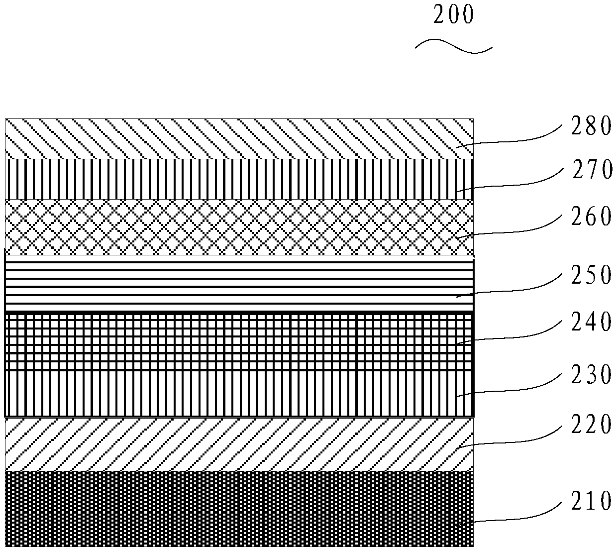
[0099] The structure of an electroluminescent device is: ITO / PEDOT:PSS / PVK / mCP:Ag 2 Cl 2 (dppb) 2 :(CdSe / ZnS quantum rod) / PO-T2T / LiF / Al.
[0100] The preparation method of the above-mentioned electroluminescent device is basically the same as that of Example 1, except that the preparation method of the electroluminescent layer is different, specifically: the ink of the electroluminescent layer contains 8 mg / mL of mCP, 8 mg / mL of Ag 2 Cl 2 (dppb) 2 and 16mg / mL CdSe / ZnS quantum rods.
PUM
| Property | Measurement | Unit |
|---|---|---|
| Luminous wavelength | aaaaa | aaaaa |
| Thickness | aaaaa | aaaaa |
Abstract
Description
Claims
Application Information
 - R&D
- Intellectual Property
- Life Sciences
- Materials
- Tech Scout
- Unparalleled Data Quality
- Higher Quality Content
- 60% Fewer Hallucinations
Browse by: Latest US Patents, China's latest patents, Technical Efficacy Thesaurus, Application Domain, Technology Topic, Popular Technical Reports.
© 2025 PatSnap. All rights reserved.Legal|Privacy policy|Modern Slavery Act Transparency Statement|Sitemap|About US| Contact US: help@patsnap.com