Composite multilayer thin film material with optical property and rectification effect, and preparation method and application thereof
A multi-layer film and rectification effect technology, applied in the field of photocatalytic materials, achieves the effects of high processing temperature, strong light absorption performance, and simple operation
- Summary
- Abstract
- Description
- Claims
- Application Information
AI Technical Summary
Problems solved by technology
Method used
Image

Examples
Embodiment 1
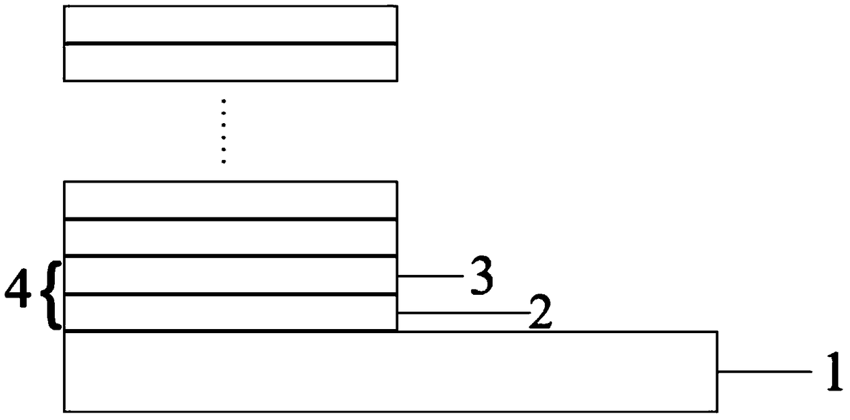
[0051] see figure 1 , is a schematic structural view of the composite multilayer thin film material in the embodiment of the present invention. The present embodiment carries out the preparation of composite multi-layer film material of the present invention, comprises the following steps:
[0052] (1) Substrate 1 of the present embodiment is a layer of F-doped SnO coated on the surface of soda-lime glass. 2 The FTO conductive glass is a transparent substrate. Firstly, the substrate 1 is cleaned with deionized water, acetone, ethanol and deionized water in sequence, and then blown dry with nitrogen gas. The cleaning time is 15 minutes each time.
[0053] (2) Carry out CuCrO to the cleaned substrate 1 2 For the deposition of film 2, put the substrate 1 into the substrate tray and put it into the sputtering chamber, vacuumize the sputtering chamber, and use the FJL-560 magnetron sputtering machine to conduct CuCrO 2 Preparation of Film 2. Pre-sputtering was carried out for ...
Embodiment 2
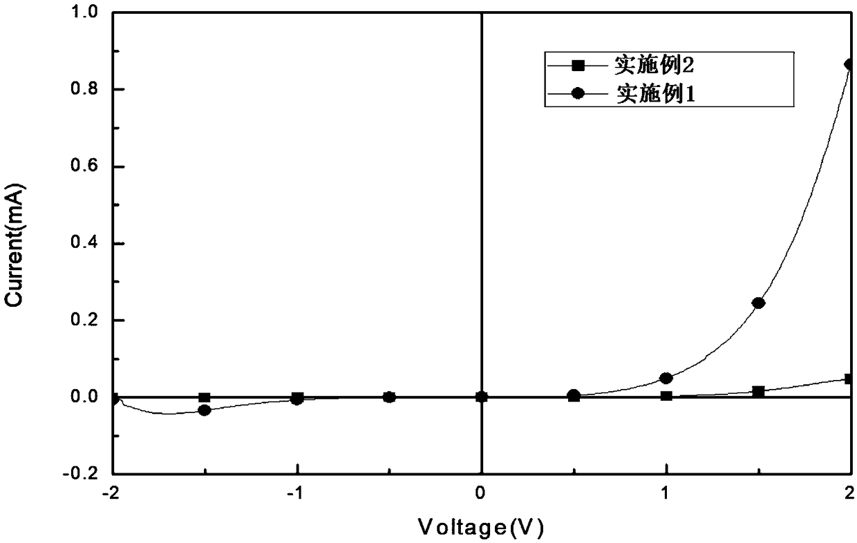
[0057] This embodiment changes the time and modulation period of magnetron sputtering on the basis of embodiment 1, CuCrO 2 The sputtering time for the deposition of film 2 was 8.5 min, and the sputtering time for the deposition of CuO film 3 was 8.5 min. The sputtering was repeated 6 times in total, and the cycle of alternate deposition was 6 cycles. In the prepared composite multilayer film material, CuCrO 2 The thickness ratio of film 2 and CuO film 3 is 1:2, and each layer of CuCrO 2 The thickness of the thin film 2 is 11.1 nm, and the thickness of each CuO thin film 3 is 22.2 nm.
Embodiment 3
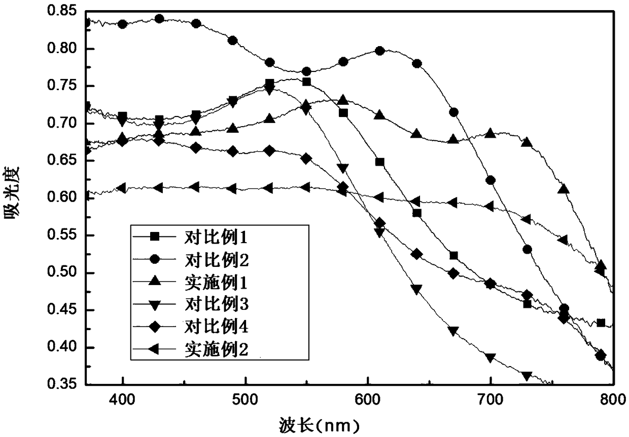
[0067] In this embodiment, the composite multilayer film material of the embodiment and the composite multilayer film material of the comparative example are tested for ultraviolet-visible light absorption spectrum. For the results, please refer to figure 2 , are the ultraviolet-visible light absorption spectra of the composite multilayer thin film material of the embodiment of the present invention and the composite multilayer thin film material of the comparative example. The results show that both the composite multilayer film material of Example 1 and the composite multilayer film material of Example 2 have good and stable absorbance, and the absorption peaks are around 711nm and 707nm respectively. The light absorption peaks of the composite multilayer film material of comparative example 1, the composite multilayer film material of comparative example 2 and the composite multilayer film material of comparative example 3 are at about 542nm, 617nm and 520nm respectively, a...
PUM
| Property | Measurement | Unit |
|---|---|---|
| thickness | aaaaa | aaaaa |
| thickness | aaaaa | aaaaa |
Abstract
Description
Claims
Application Information
 - R&D Engineer
- R&D Manager
- IP Professional
- Industry Leading Data Capabilities
- Powerful AI technology
- Patent DNA Extraction
Browse by: Latest US Patents, China's latest patents, Technical Efficacy Thesaurus, Application Domain, Technology Topic.
© 2024 PatSnap. All rights reserved.Legal|Privacy policy|Modern Slavery Act Transparency Statement|Sitemap