Optical element defect detection method based on machine vision technology

A defect detection and optical component technology, applied in the direction of optical testing of flaws/defects, material analysis by optical means, instruments, etc., can solve the problems of unstable micro-defect detection, etc., and achieve moderate price, powerful functions, and low false detection rate. Effect

Inactive Publication Date: 2018-12-18
大连鉴影光学科技有限公司
View PDF15 Cites 30 Cited by
  • Summary
  • Abstract
  • Description
  • Claims
  • Application Information

AI Technical Summary

Problems solved by technology

[0009] The present invention mainly solves the technical problem that the micro-defects cannot be detected stably in the prior art, and proposes a defect detection method for optical components based on machine vision technology, which uses the alternating change of the gray value of the light source to realize high-quality defect detection, and at the same time It can stably detect minor defects and replace manual inspection

Method used


Image

  • Optical element defect detection method based on machine vision technology
  • Optical element defect detection method based on machine vision technology
  • Optical element defect detection method based on machine vision technology

Examples


Embodiment 1

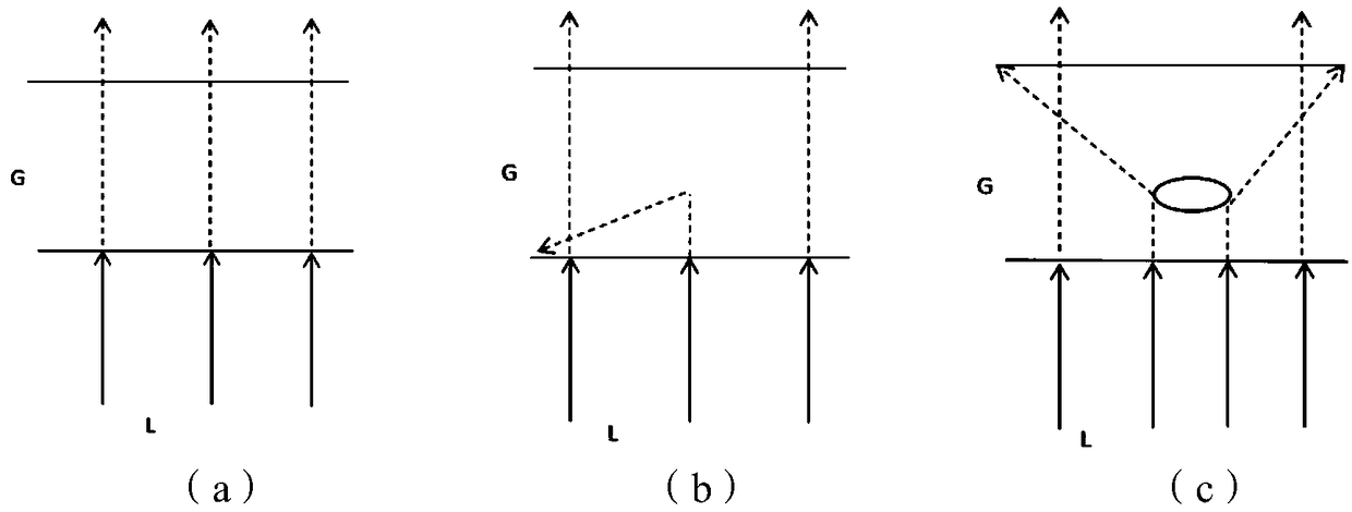
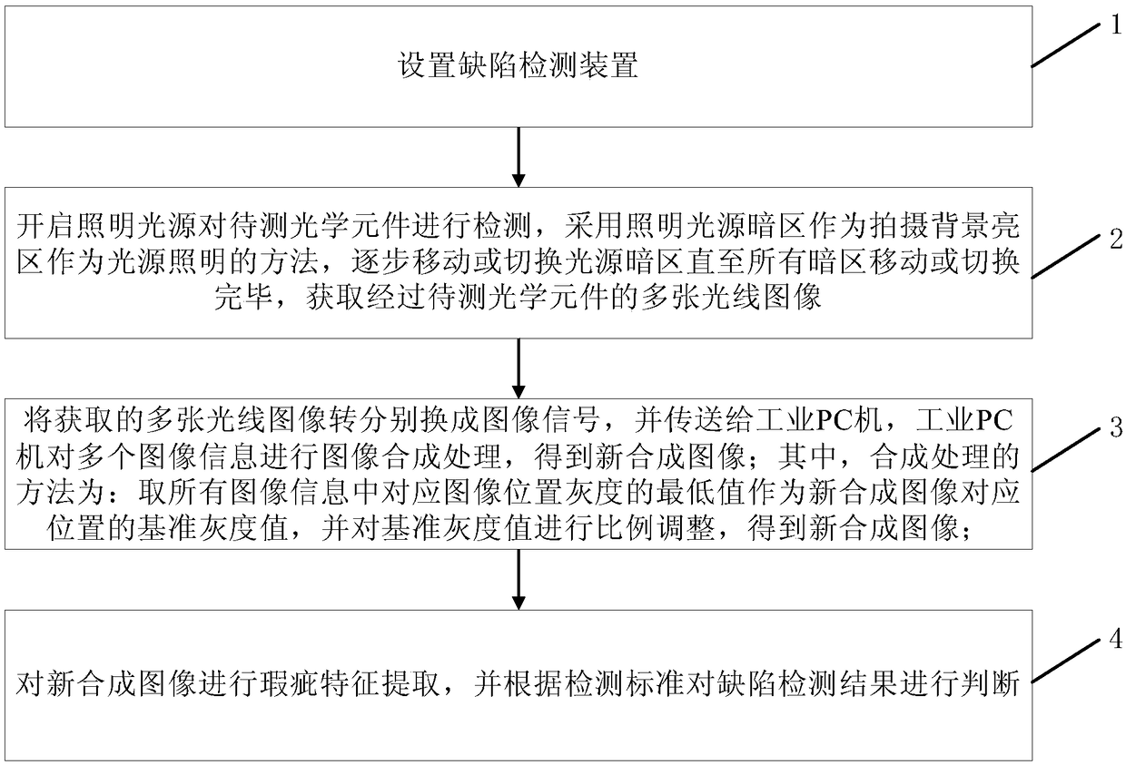
[0036] figure 2 It is a flow chart of the implementation of the optical element defect detection method based on machine vision technology of the present invention. This embodiment describes the detection of transmission defects, such as figure 2 As shown, the optical component defect detection method based on machine vision technology provided by the embodiment of the present invention includes:

[0037] Step 1, setting up a defect detection device.

[0038] This embodiment is used for transmission-type defect detection. The illumination source and the image acquisition device are respectively located on both sides of the object to be tested. The image acquisition device can observe the image of the transmitted illumination source through the optical element under test.

[0039] The defect detection equipment in this embodiment includes: an illumination source, an image acquisition device, and an industrial PC. The image acquisition device observes the image of the transm...

Embodiment 2

[0068] This embodiment is basically consistent with Embodiment 1, the difference is:

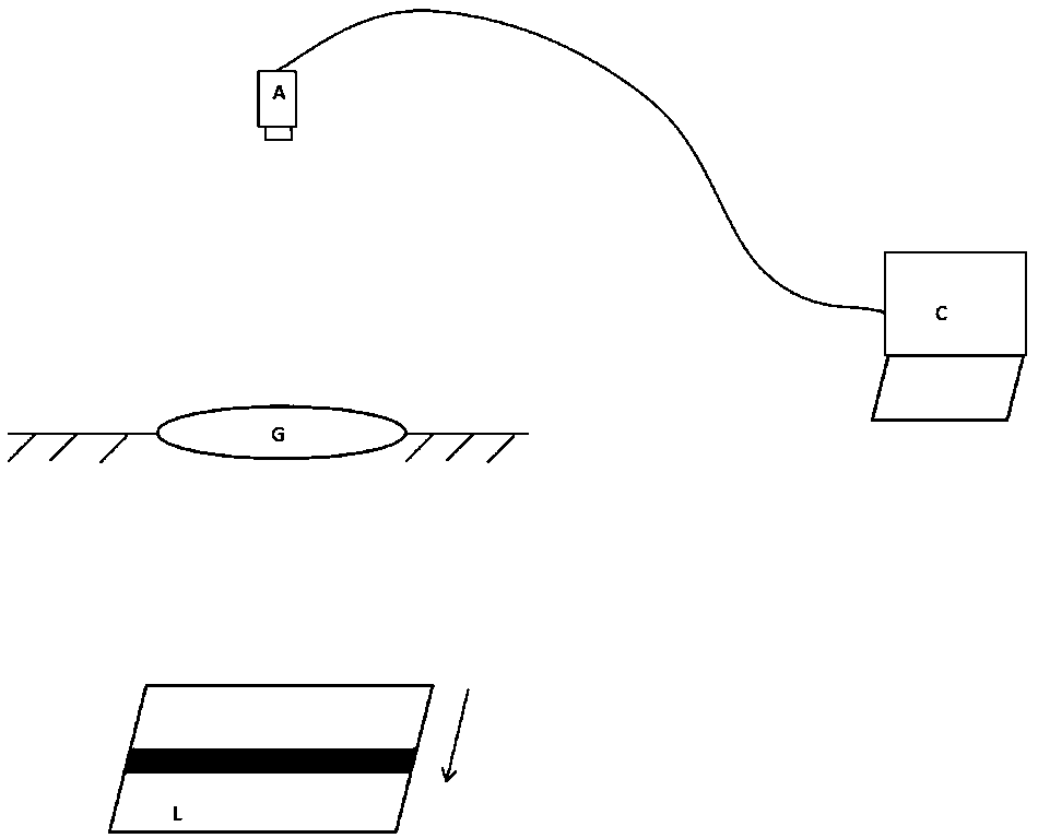
[0069] This embodiment is used to detect reflective defects, such as Figure 9 As shown, in step 1, the defect detection device is set up, the illumination source and the image acquisition device are respectively located on the same side of the object to be tested, and the light source is reflected to the image acquisition device through the object to be tested, and the image acquisition device can observe through the optical element under test to the image of the reflected illumination source. What is obtained in step 2 is the reflected ray image.

[0070] At the same time, in order to improve the speed of detection, the lighting source can be used such as Figure 4 As shown, that is, the black and white checkerboard replaces the transformation method instead of the horizontal or vertical dark field stripe scanning method. In this method, the industrial camera only needs to collect two im...

Embodiment 3

[0072] This embodiment is basically consistent with Embodiment 1, the difference is:

[0073] This embodiment is used to detect optical elements with special shapes, such as optical elements with a certain R value, such as Figure 10 As shown, the dark-field lighting source is located at the focal length of the object under test, and the industrial camera only needs to collect one image to analyze the defects of the object under test.


PUM


Abstract

The invention relates to the field of optical element detection, and provides an optical element defect detection method based on machine vision technology, comprising the following steps of: step 1,setting a defect detection device; step 2, turning on an illuminating light source to detect the optical element to be detected, and gradually moving or switching dark regions of the light source until all dark regions are completely moved or switched to acquire a plurality of light images passing through the optical element to be detected by adopting the dark regions of the illumination light source as a shooting background and the bright regions as a light source to illuminate; step 3, converting the plurality of acquired light images into image signals, and transmitting the image signals toan industrial PC, wherein the industrial PC performs image synthesis processing on the information of the plurality of images to acquire a new composite image; and step 4, performing defect feature extraction on the new composite image, and judging a defect detection result according to the detection standard. The optical element defect detection method based on machine vision technology realizesthe high-quality defect detection using alternating changes in gray values of the light source, and can stably detect slight defects and replace the manual detection.

Description

technical field [0001] The invention relates to the field of optical element detection, in particular to a method for detecting optical element defects based on machine vision technology. Background technique [0002] Due to the limitations of modern processing technology, various defects will inevitably be left on the surface of precision optical components during the processing process. These defects generally refer to pits, scratches, open air bubbles and Broken edges etc. In practical applications, the defects on the surface of optical components cause light scattering to be much stronger than other types of scattering in some cases, causing energy absorption to the components, harmful flaunting, diffraction patterns, film damage, and laser damage Wait. Therefore, waste products that do not meet the standards must be detected through strict testing procedures. [0003] Manual inspection is mainly based on subjective consciousness and past experience to distinguish and...

Claims


Application Information

Patent Timeline
Patent Type & Authority Applications(China)
IPC IPC(8): G01N21/88
CPCG01N21/8851G01N2021/8887
Inventor 郭右利王芳
Owner 大连鉴影光学科技有限公司
Why Eureka
Try Eureka