Multi-sampling CMOS image sensor pixel structure and ultra-high speed image acquisition method thereof
A technology of image sensor and pixel structure, which is applied in image communication, electrical components, television, etc., can solve the problems of poor imaging performance, complex process, high cost, etc., and achieve the goal of small process change, low implementation difficulty, and reduced development cost Effect
- Summary
- Abstract
- Description
- Claims
- Application Information
AI Technical Summary
Problems solved by technology
Method used
Image

Examples
Embodiment Construction
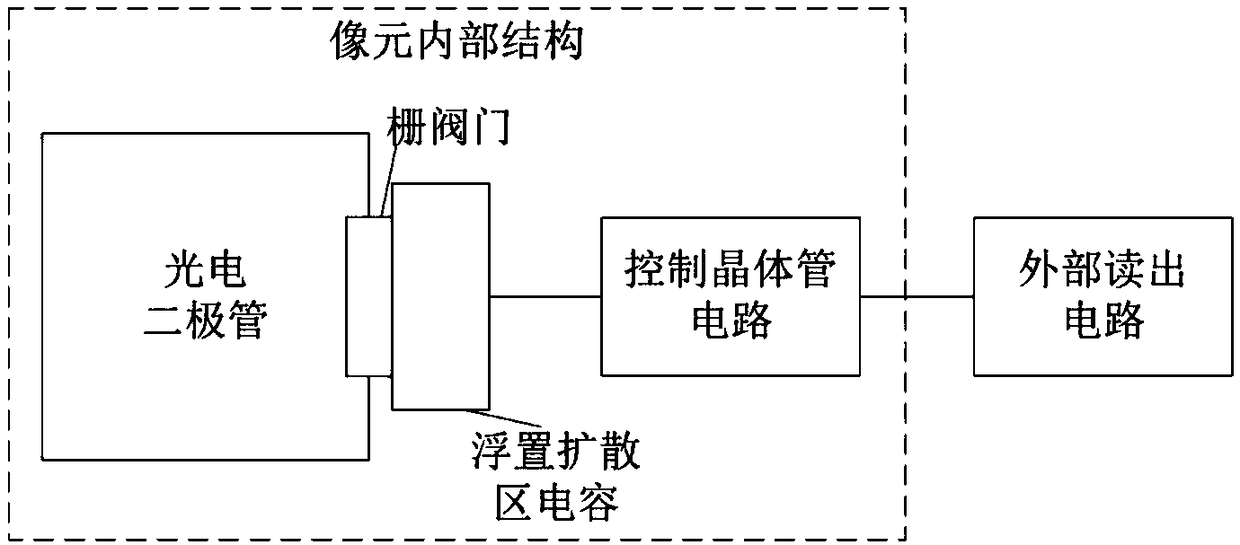
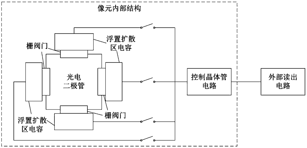
[0036] Multi-sampling CMOS image sensor pixel structure provided by the present invention, and figure 1 The traditional CMOS image sensor pixel structure shown is different in that a photodiode in the present invention is connected to multiple control switch tubes and multiple floating diffusion area capacitors, and can sample and buffer the image signals generated by the photodiode in time-sharing to obtain Multiple high-time-resolved image data.
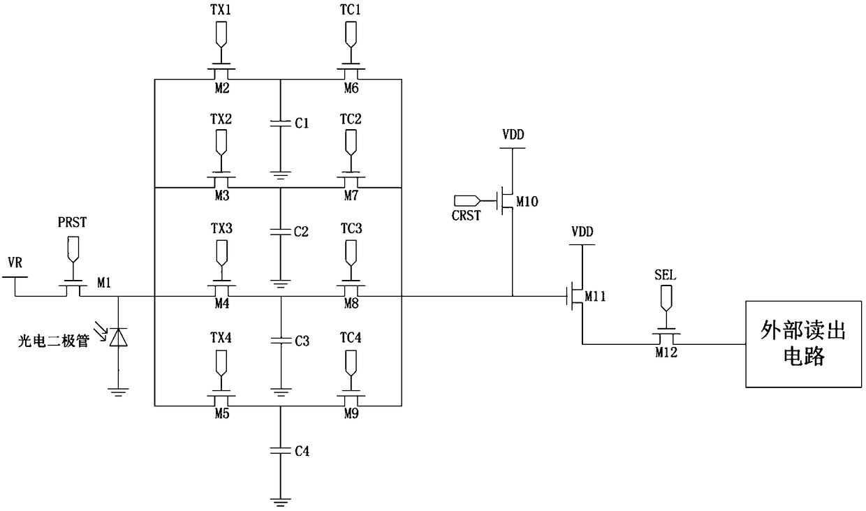
[0037] Take four-port sampling CMOS image sensor pixel structure model as example below, the present invention is described in detail:
[0038] Such as figure 2 As shown, the four gate valves are evenly distributed around the photodiode, and each gate valve is connected to a floating diffusion area capacitor. The four floating diffusion area capacitors share a control transistor circuit and are controlled by four charge output gating switches. The time-division transmission of the capacitor buffer signal in the floating diffusio...
PUM
 Abstract
Description
Claims
Application Information
 - Generate Ideas
- Intellectual Property
- Life Sciences
- Materials
- Tech Scout
- Unparalleled Data Quality
- Higher Quality Content
- 60% Fewer Hallucinations
Browse by: Latest US Patents, China's latest patents, Technical Efficacy Thesaurus, Application Domain, Technology Topic, Popular Technical Reports.
© 2025 PatSnap. All rights reserved.Legal|Privacy policy|Modern Slavery Act Transparency Statement|Sitemap|About US| Contact US: help@patsnap.com