A kind of optical fiber lead-out method for photonic chip

A technology of photonic chips and optical fibers, applied in the field of optical fiber devices, to achieve the effect of active connection, suitable for mass production, and improve the efficiency of light extraction and coupling

Active Publication Date: 2020-07-03
华能(泰安)光电科技有限公司
View PDF10 Cites 0 Cited by
  • Summary
  • Abstract
  • Description
  • Claims
  • Application Information

AI Technical Summary

Problems solved by technology

[0007] The object of the present invention is to provide a method for extracting optical fibers used in micro-opto-electromechanical systems or photonic chips, so as to solve at least one technical problem in the prior art

Method used


Image

  • A kind of optical fiber lead-out method for photonic chip
  • A kind of optical fiber lead-out method for photonic chip
  • A kind of optical fiber lead-out method for photonic chip

Examples


Embodiment

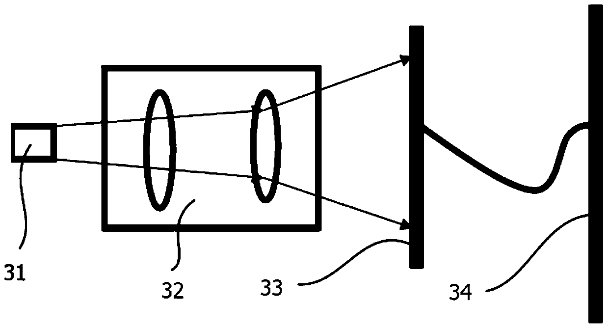
[0040] Such as image 3 As shown, a camera display system is provided, including: an optical magnification system 32, a camera target surface 33, an image processing system and a display 34;

[0041] Measure the position of the camera target surface 33 in advance, and mark a straight line parallel to the camera target surface 33 on the six-dimensional adjustment frame;

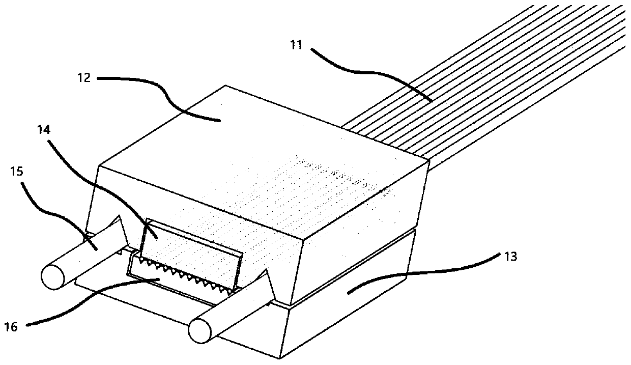
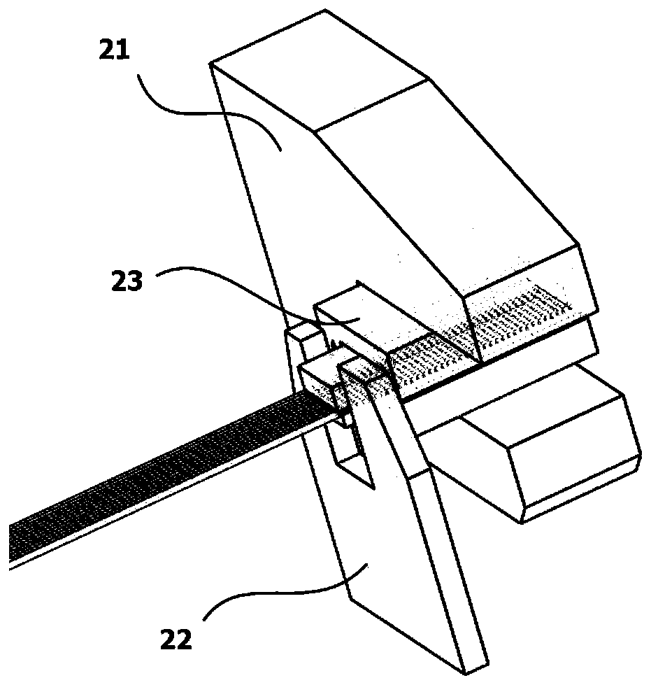
[0042] Further, a standard multi-core connector 23 with guide pin holes, such as figure 2 As shown, the photonic chip 51 is clamped by the fixture 41 and installed on the six-dimensional adjustment frame, and an optical amplification system 32 and a camera are placed, so that the end face of the multi-core connector 23 with guide pin holes can be photographed;

[0043] Further, adjust the six-dimensional adjustment frame to adjust the six degrees of freedom of left and right, front and rear, up and down, rotation, pitch, and swing respectively, so that the multi-core connector 23 with guide pin holes is para...


PUM


Abstract

The invention discloses an optical fiber leading method for a photon chip. According to the optical fiber leading method, the photon chip, a guide pin structural body and a multi-core connector are provided; the multiple optical waveguide end faces of the photon chip and the end face of the guide pin structural body are imaged and shot through a wide-view optical amplification system or a large-area camera target surface and a high-quantity photosensitive element dot matrix; the relative positions of multiple optical waveguides of the photo chip and the guide pin structural body are adjusted through an adjusting rack, and positioning and adjusting are conducted according to a standard template; bonding fixation is conducted through a bonding agent after positioning and adjusting, and a photon chip connector is obtained; positioning and bonding fixation of an optical fiber array and the guide pin structural body are completed through the same method, and an optical fiber array connectoris obtained; the photon chip connector or the optical fiber array connector is provided with a guide pin, the photon chip connector and the optical fiber array connector are in butt joint, positioning is conducted through the guide pin and a guide pin hole, and optical fiber leading of the photon chip is achieved.

Description

technical field [0001] The invention relates to the fields of optical fiber devices and the like, in particular to an optical fiber extraction method for a photonic chip. Background technique [0002] Photonic chips include micro-opto-electromechanical systems, silicon photonic chips, planar waveguide chips, etc., which are widely used in optical communications, sensors and computers. The photonic chip can realize functions such as branching, wavelength division multiplexing, phase modulation, and photoelectric detection. The waveguide on the photonic chip is aligned and coupled with the optical fiber, and packaged to realize the extraction of the optical fiber. Photon chip. [0003] At present, the lead-out of the photonic chip needs to adjust the relative position of the fiber array and the photonic chip through a six-dimensional adjustment frame, and detect it through light until the insertion loss is minimized, and then fix the relative position of the fiber array and t...

Claims


Application Information

Patent Timeline
Patent Type & Authority Patents(China)
IPC IPC(8): G02B6/36
CPCG02B6/3616G02B6/364
Inventor 谷丽芳
Owner 华能(泰安)光电科技有限公司
Why Eureka
Try Eureka