Nanoimprint replica mold, manufacturing method therefor, and nanoimprint replica mold manufacturing device

A technology of nanoimprinting and transfer printing, which is applied in the direction of nanostructure manufacturing, photolithographic process exposure device, nanotechnology, etc., which can solve the problems of high manufacturing unit price, complicated manufacturing process, and low pattern accuracy, and achieve low manufacturing unit price and high manufacturing efficiency. The effect of simple process and improved precision

Inactive Publication Date: 2018-12-21
GIGALANE CO LTD
View PDF9 Cites 2 Cited by
  • Summary
  • Abstract
  • Description
  • Claims
  • Application Information

AI Technical Summary

Problems solved by technology

[0005] However, the conventional replica mold 1 is made of metal materials such as nickel (Ni) and copper (Cu), so there are problems of low pattern accuracy, complicated manufacturing process, and high manufacturing unit price.

Method used


Image

  • Nanoimprint replica mold, manufacturing method therefor, and nanoimprint replica mold manufacturing device
  • Nanoimprint replica mold, manufacturing method therefor, and nanoimprint replica mold manufacturing device
  • Nanoimprint replica mold, manufacturing method therefor, and nanoimprint replica mold manufacturing device

Examples


Embodiment Construction

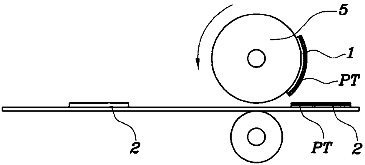
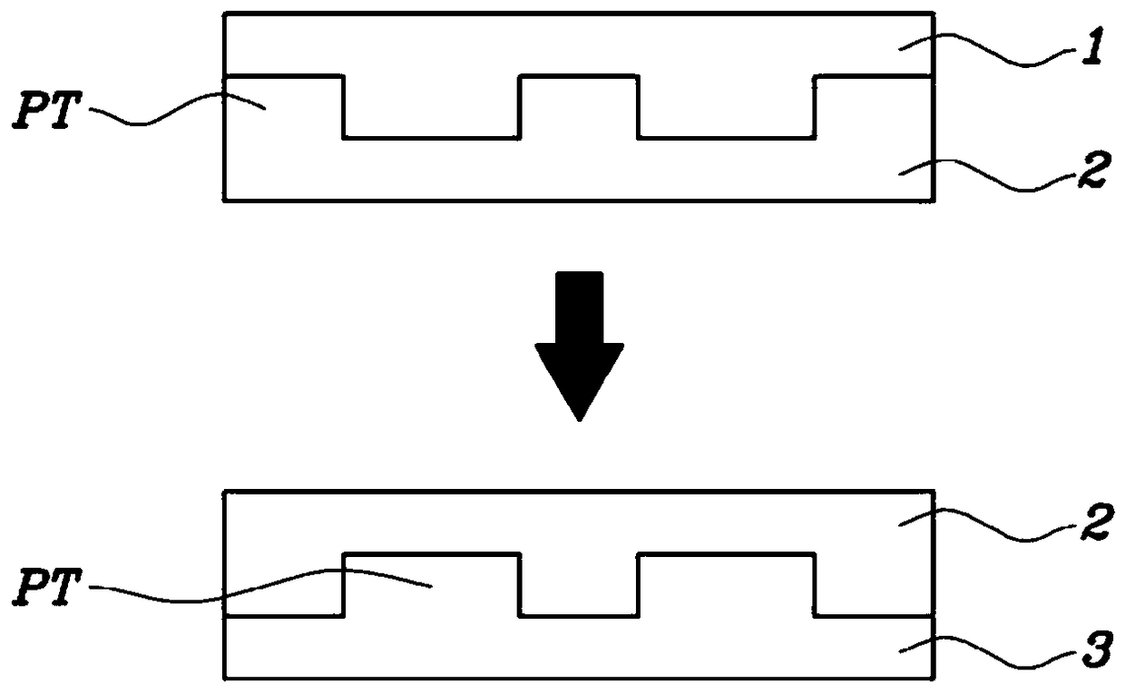
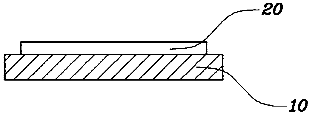
[0026] The purpose, specific advantages and new features of the present invention will become easier to understand in the following detailed description and embodiments described in conjunction with the accompanying drawings. It should be noted that, when assigning reference numerals to constituent elements in each figure in this specification, even if the same constituent elements are indicated in different drawings, the same numerals should be assigned as much as possible. Also, although the terms first, second, etc. may be used to describe various constituent elements, the constituent elements are not limited to the terms. The terms are used only for the purpose of distinguishing one constituent element from another constituent element. In addition, in describing the present invention, when it is judged that the specific description of the related known technology would unnecessarily obscure the gist of the present invention, the detailed description will be omitted.

[00...


PUM


Abstract

Disclosed are a nanoimprint replica mold, a manufacturing method therefor, and a nanoimprint replica mold manufacturing device. The nanoimprint replica mold of the present invention comprises: a basemade of a plastic film; a stamping unit formed in the base; and a guide film separably formed in the base, having a hollow portion such that the stamping unit can be exposed, and having particles formed by the spreading and curing of the outer circumferential surface of the stamping unit, wherein the stamping unit is made of resin and has an uneven shape pattern.

Description

technical field [0001] The present invention relates to a replica mold for nanoimprinting, a manufacturing method thereof, and a manufacturing device for a replica mold for nanoimprinting. Background technique [0002] The nanoimprint process is a technology that replaces the photoresist (photoresist) to form a pattern (pattern) on the substrate (substrate). A process in which a patterned stamping die transfers (stamps) the resin on the upper portion of the substrate to form a pattern on the upper portion of the substrate. [0003] At this time, the pattern of the stamping mold used in the nanoimprint process is formed by transferring the pattern of the replica mold. [0004] Usually, such as figure 1 As shown in the figure, when the stamping die 2 passes through the roll 5 of the roll-to-roll (roll to roll) equipment to which the replica mold 1 formed with the pattern PT is attached, the pattern PT of the replica mold 1 is transferred to the stamping die 2 for stamping. ...

Claims


Application Information

Patent Timeline
Patent Type & Authority Applications(China)
IPC IPC(8): G03F7/16G03F7/00B29C43/02B29C35/08B29C33/60G03F7/20H01L21/027H01L29/06B82B3/00
CPCB29C33/60B29C35/08B29C43/02B82B3/00G03F7/00G03F7/16G03F7/20H01L21/027H01L29/06B29C35/0888B29C43/021G03F7/0002G03F7/161G03F7/2012H01L21/0274H01L29/0665
Inventor 权相民具滋鹏丘璜燮金铉济郑熙锡
Owner GIGALANE CO LTD
Why Eureka
Try Eureka