Chip on film substrate, display panel and preparation method thereof, and display device

A chip-on-chip and display panel technology, applied in optics, instruments, electrical components, etc., can solve problems such as low production efficiency and complicated process

Active Publication Date: 2019-01-04
BOE TECH GRP CO LTD +1
View PDF9 Cites 2 Cited by
  • Summary
  • Abstract
  • Description
  • Claims
  • Application Information

AI Technical Summary

Problems solved by technology

As a result, the process is complicated and the production efficiency is low

Method used


Image

  • Chip on film substrate, display panel and preparation method thereof, and display device
  • Chip on film substrate, display panel and preparation method thereof, and display device
  • Chip on film substrate, display panel and preparation method thereof, and display device

Examples


Embodiment Construction

[0032] Embodiments of the present invention are described in detail below, examples of which are shown in the drawings, wherein the same or similar reference numerals designate the same or similar elements or elements having the same or similar functions throughout. The embodiments described below by referring to the figures are exemplary only for explaining the present invention and should not be construed as limiting the present invention.

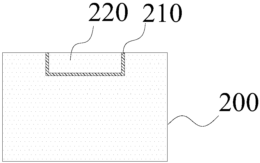
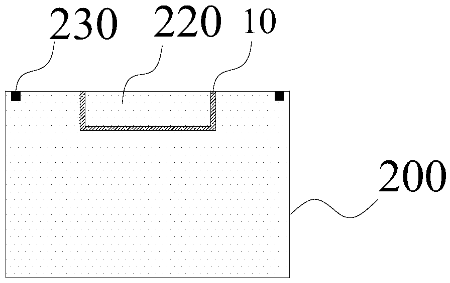
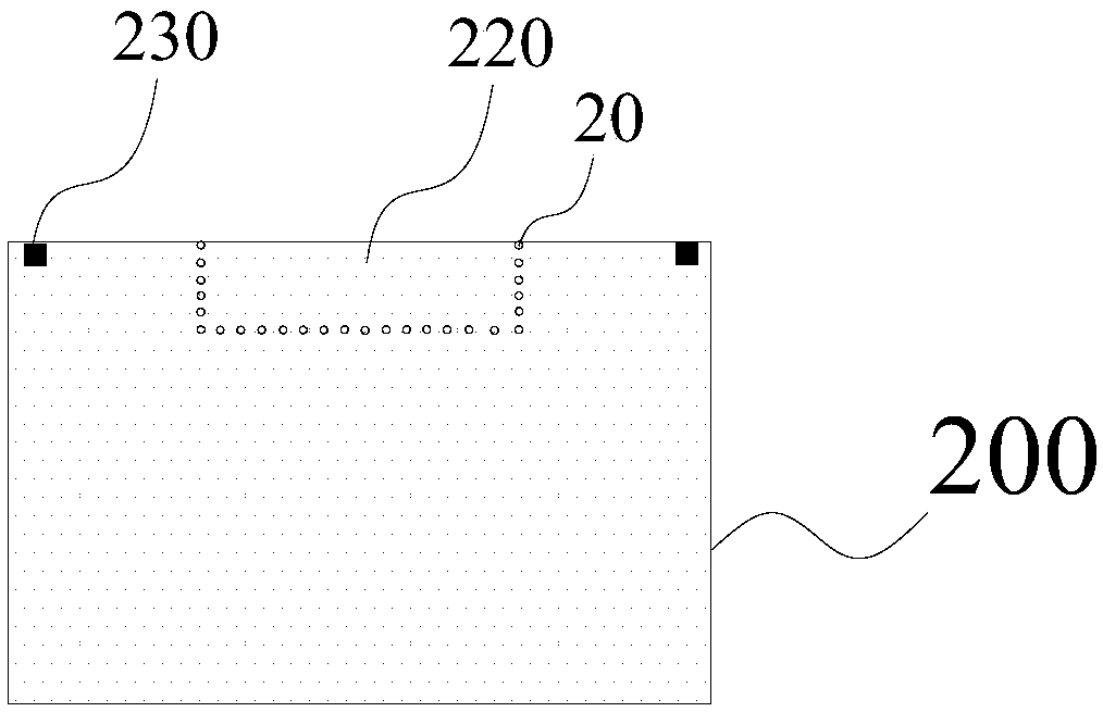
[0033] In one aspect of the present invention, the present invention provides a chip-on-film substrate. According to an embodiment of the present invention, refer to figure 1, the edge of the chip-on-film substrate 200 has a cutting mark 210 , and the cutting mark 210 defines a trench area 220 at the edge of the chip-on-film substrate 200 . Before the chip-on-film substrate is fixed to the display module and forms the display panel, no grooves are pre-formed, thus avoiding the problem that the two edges of the grooves need to be positi...


PUM


Abstract

The invention discloses a chip on film substrate, a display panel and a preparation method thereof, and a display device. According to the embodiment of the invention, the edge of the chip on film substrate is provided with a cut mark, wherein the cut mark defines a trenching area at the edge of the chip on film substrate. Thus, when the display panel is formed by using the chip on film substrate,the chip on film substrate can be fixed to a substrate of a display module by only one alignment, and the process is simple and the production efficiency is high; and moreover, the alignment accuracyis high, and the dislocation problem caused by corner warping of the trenching area in the alignment process is avoided, the product yield is improved, and the product adverse risk is reduced.

Description

technical field [0001] The present invention relates to the field of display technology, in particular to a chip-on-chip film substrate, a display panel, a preparation method thereof, and a display device. Background technique [0002] With the advent of the "full screen" era, high screen-to-body ratio display devices are favored by consumers, which poses new challenges to the structural design of display panels. At present, due to the limitation of the gate array (Gate on Array, GOA) drive unit, the design of the left and right borders of the full-screen display panel has reached the technological limit, but the design of the upper and lower borders of the display panel still has a lot of room for development. In order to realize the display panel The upper and lower narrow frame design, the COF (Chip on flexible printed circuit) process gradually replaces the traditional COG (Chip on glass) process, and becomes the direction of future display panel development. Specifical...

Claims


Application Information

Patent Timeline
Patent Type & Authority Applications(China)
IPC IPC(8): G02F1/1333H01L23/544
CPCG02F1/1333G02F1/133351H01L23/544H01L2223/54426
Inventor 韩帅王跃林徐敬义张慧杰郭智昂石天雷
Owner BOE TECH GRP CO LTD
Why Eureka
Try Eureka