Single photon avalanche diode detector with echelle grating structure and manufacturing method

A single-photon avalanche and echelle grating technology, which is applied in semiconductor devices, final product manufacturing, sustainable manufacturing/processing, etc., can solve the problems of low near-infrared short-wave photon efficiency, improve photon detection efficiency, increase photon generation rate, The effect of low power consumption

Active Publication Date: 2020-10-02
武汉光迹融微科技有限公司
View PDF13 Cites 0 Cited by
  • Summary
  • Abstract
  • Description
  • Claims
  • Application Information

AI Technical Summary

Problems solved by technology

[0003] Purpose of the invention: In view of the low efficiency of traditional CMOS SPAD detectors in detecting near-infrared short-wave photons, the present invention proposes a single-photon avalanche diode detector with an echelon grating structure

Method used


Image

  • Single photon avalanche diode detector with echelle grating structure and manufacturing method
  • Single photon avalanche diode detector with echelle grating structure and manufacturing method
  • Single photon avalanche diode detector with echelle grating structure and manufacturing method

Examples


Embodiment Construction

[0023] The present invention will be further described in detail below in conjunction with the accompanying drawings.

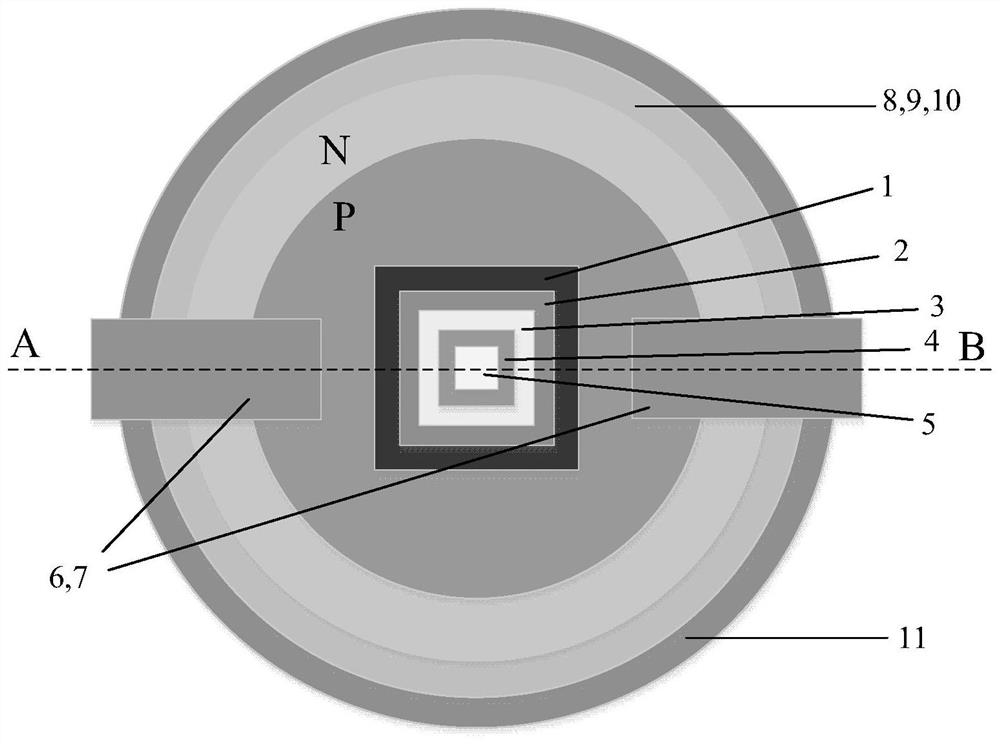
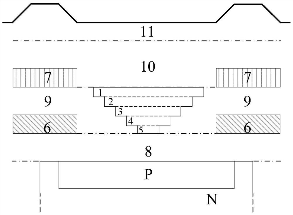
[0024] Such as figure 1 and figure 2 As shown, the SPAD detector of the present invention includes an active region, an inner layer dielectric region 8 , a metal isolation dielectric region 9 , a top dielectric region 10 and a passivation layer 11 from bottom to top in a vertical direction. The active region is located inside the substrate and includes an N-type active region and a P-type active region arranged at the center above the N-type interior. The upper surface of the N-type active region surrounds the upper surface of the P-type active region and is in contact with the substrate. The upper surface of the bottom is flush. The depletion region formed between the P-type active region and the N-type active region is the avalanche detection region of the single photon avalanche diode. The metal isolation dielectric region 9 is provided with the first ...


PUM


Abstract

The invention discloses a single-photon avalanche diode detector with a step grating structure and a manufacturing method thereof. The diode detector comprises an active region, an inner layer dielectric region, a metal isolation dielectric region and a top dielectric region in order from bottom to top in a vertical direction. The metal isolation dielectric region is provided with a first metal interconnection region and a step grating structure; The top dielectric region is provided with a second metal interconnection region; The first metal interconnect region and the second metal interconnect region do not obstruct the step grating structure in the vertical direction. The invention increases the photon generation rate of the avalanche region in the active region by introducing a five-step grating structure into the metal isolation medium region through the diffraction effect of light, thereby further improving the photon detection efficiency of the device and enhancing the ability of the device to detect near-infrared photons. These detectors can be fabricated in standard CMOS process, and have the advantages of high integration, low power consumption, strong anti-interference ability and so on.

Description

technical field [0001] The invention relates to a single photon avalanche diode detector and a manufacturing method, in particular to a single photon avalanche diode detector with an echelle grating structure and a manufacturing method. Background technique [0002] Single-photon avalanche diode (SPAD) detectors have the advantages of high detection efficiency, fast response speed, and low power consumption, and have been widely used in biomedicine, military, and optical communications. SPAD detectors based on CMOS technology can integrate SPAD devices and quenching, counting, and readout circuits into one chip, thereby realizing low-cost, high-integration, and high-reliability array detectors. However, in specific application fields such as distance measurement, fluorescence lifetime analysis, optical tomography, and optical fiber communication, in order to avoid the damage of the laser light source of the SPAD detector to the human eye, the laser wavelength is generally re...

Claims


Application Information

Patent Timeline
Patent Type & Authority Patents(China)
IPC IPC(8): H01L31/107H01L31/0232H01L31/18
CPCH01L31/02327H01L31/107H01L31/18Y02P70/50
Inventor 孙飞阳徐跃吴仲
Owner 武汉光迹融微科技有限公司
Why Eureka
Try Eureka