A power device and a preparation method thereof

A technology of power devices and epitaxial layers, applied in the fields of semiconductor/solid-state device manufacturing, semiconductor devices, electrical components, etc., can solve the problems that affect the performance of VDMOS devices, improve the on-resistance, and is not conducive to reducing the power loss of devices, so as to improve the impact resistance. The effect of breakdown voltage capability, reduction of on-resistance, and improvement of breakdown voltage capability

Inactive Publication Date: 2019-01-08
深圳市心版图科技有限公司
View PDF3 Cites 0 Cited by
  • Summary
  • Abstract
  • Description
  • Claims
  • Application Information

AI Technical Summary

Problems solved by technology

By increasing the thickness of the epitaxial layer or reducing the doping concentration of the epitaxial layer, the breakdown voltage can be increased, but at the same time, the on-resistance is increased, which is not conducive to reducing the power loss when the device is turned on.
It can be seen that there is an unresolvable contradiction between increasing the VDMOS breakdown voltage and reducing the on-resistance in the existing technology, which affects the continuous improvement of the performance of VDMOS devices.

Method used


Image

  • A power device and a preparation method thereof
  • A power device and a preparation method thereof
  • A power device and a preparation method thereof

Examples


preparation example Construction

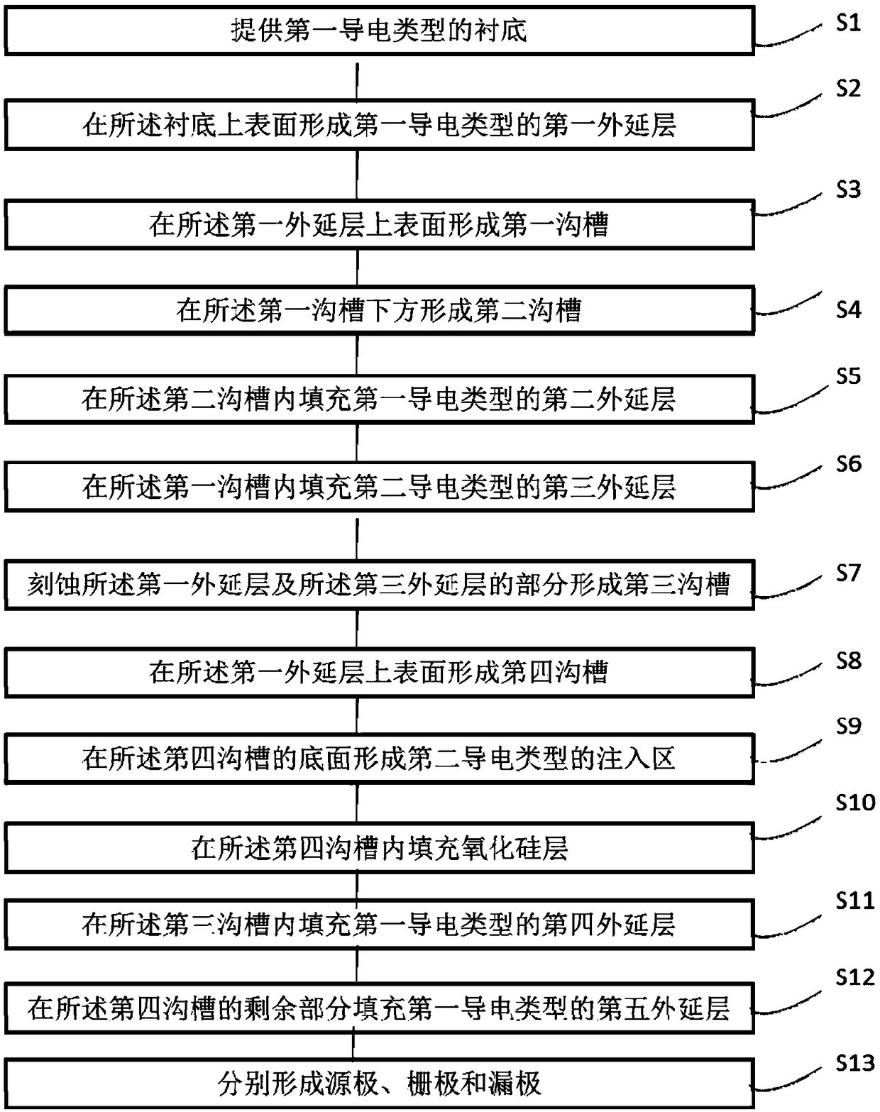
[0063] An embodiment of the present invention provides a method for preparing a power device, such as figure 1 A schematic flow chart of a method for preparing a power device provided by an embodiment shown, the method for preparing a power device includes:

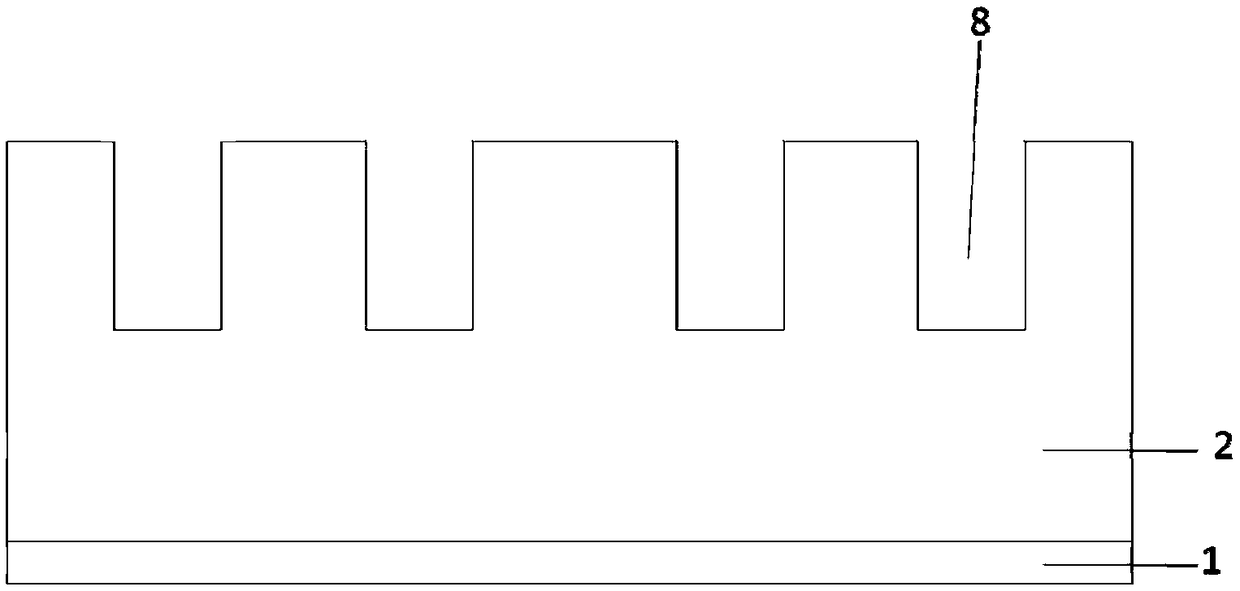
[0064] Step S1: providing a substrate 1 of the first conductivity type;

[0065] Step S2: forming a first epitaxial layer 2 of the first conductivity type on the upper surface of the substrate 1;

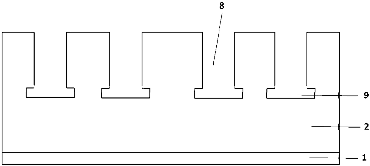
[0066] Step S3: forming first trenches 8 on the upper surface of the first epitaxial layer 2, the number of the first trenches 8 is at least two, and the number of the first trenches 8 is an even number;

[0067] Step S4: forming a second groove 9 under the first groove 8, the second groove 9 is connected to the first groove 8, and the width of the second groove 9 is larger than that of the first groove 9. the width of the trench 8;

[0068] Step S5: filling the second trench 9 with a second epitaxial layer 3 of the first co...


PUM


Abstract

A power device and a method for manufacturing the same are provided, includes a substrate of a first conductivity type, a first epitaxial layer of a first conductivity type, filling the second trenchwith a second epitaxial layer of a first conductivity type, filling the first trench with a third epitaxial layer of a second conductivity type, etching portions of the first epitaxial layer and the third epitaxial layer to form a third trench, forming an injection region of a second conductivity type on a bottom surface of the fourth trench, filling an inverted T-shaped silicon oxide layer in thefourth trench, filling a fourth epitaxial layer of the first conductivity type in the third trench, and filling a fifth epitaxial layer of the first conductivity type, a source electrode, a gate electrode, and a drain electrode in a remaining portion of the fourth trench. This structure not only increases the breakdown voltage resistance, but also decreases the on-resistance and improves the performance of VDMOS devices.

Description

technical field [0001] The invention relates to the technical field of semiconductors, in particular to a power device and a preparation method thereof. Background technique [0002] VDMOS (abbreviation of VDMOSFET, Vertical Double Diffused Metal Oxide Semiconductor Field Effect Transistor, Vertical Double Diffused Metal Oxide Semiconductor Field Effect Transistor) has drain and source poles on both sides of the device, allowing current to flow vertically inside the device, increasing the current density , the rated current is improved, and the on-resistance per unit area is also small. It is a very versatile power device. For power devices, there are two extremely important parameters, one is the on-resistance, and the other is the breakdown voltage. For the application, the on-resistance should be as small as possible, and the higher the breakdown voltage, the better. In order to withstand high voltages, power devices need to use very thick low-doped epitaxial layers. By...

Claims


Application Information

Patent Timeline
Patent Type & Authority Applications(China)
IPC IPC(8): H01L29/06H01L21/336H01L29/78
CPCH01L29/0615H01L29/66712H01L29/7802
Inventor 不公告发明人
Owner 深圳市心版图科技有限公司
Why Eureka
Try Eureka