Semiconductor device and method of manufacturing the same

a semiconductor and semiconductor technology, applied in the field of semiconductor devices, can solve the problems of crystal defect, lowering of breakdown voltage, deterioration of transistor characteristics in the application of high current, etc., and achieve the effect of high breakdown voltage performance of transistors

Inactive Publication Date: 2006-03-02
HITACHI LTD
View PDF2 Cites 2 Cited by
  • Summary
  • Abstract
  • Description
  • Claims
  • Application Information

AI Technical Summary

Benefits of technology

[0013] According to the present invention it is possible to provide a heterobipolar transistor capable of suppressing an abrupt lowering of current gain and cut-off frequency in the application of a high current while maintaining a high breakdown voltage performance of the transistor.

Problems solved by technology

As described above, in what is called a double heterobipolar transistor having two heterointerfaces, the deterioration of transistor characteristics in the application of a high current has been an unavoidable problem.
However, an increase of collector concentration causes a lowering of breakdown voltage and an increase in thickness of the silicon-germanium layer is likely to cause crystal defect due to accumulation of strain.
Thus, any of those methods cannot be the best solution.

Method used


Image

  • Semiconductor device and method of manufacturing the same
  • Semiconductor device and method of manufacturing the same
  • Semiconductor device and method of manufacturing the same

Examples


first embodiment

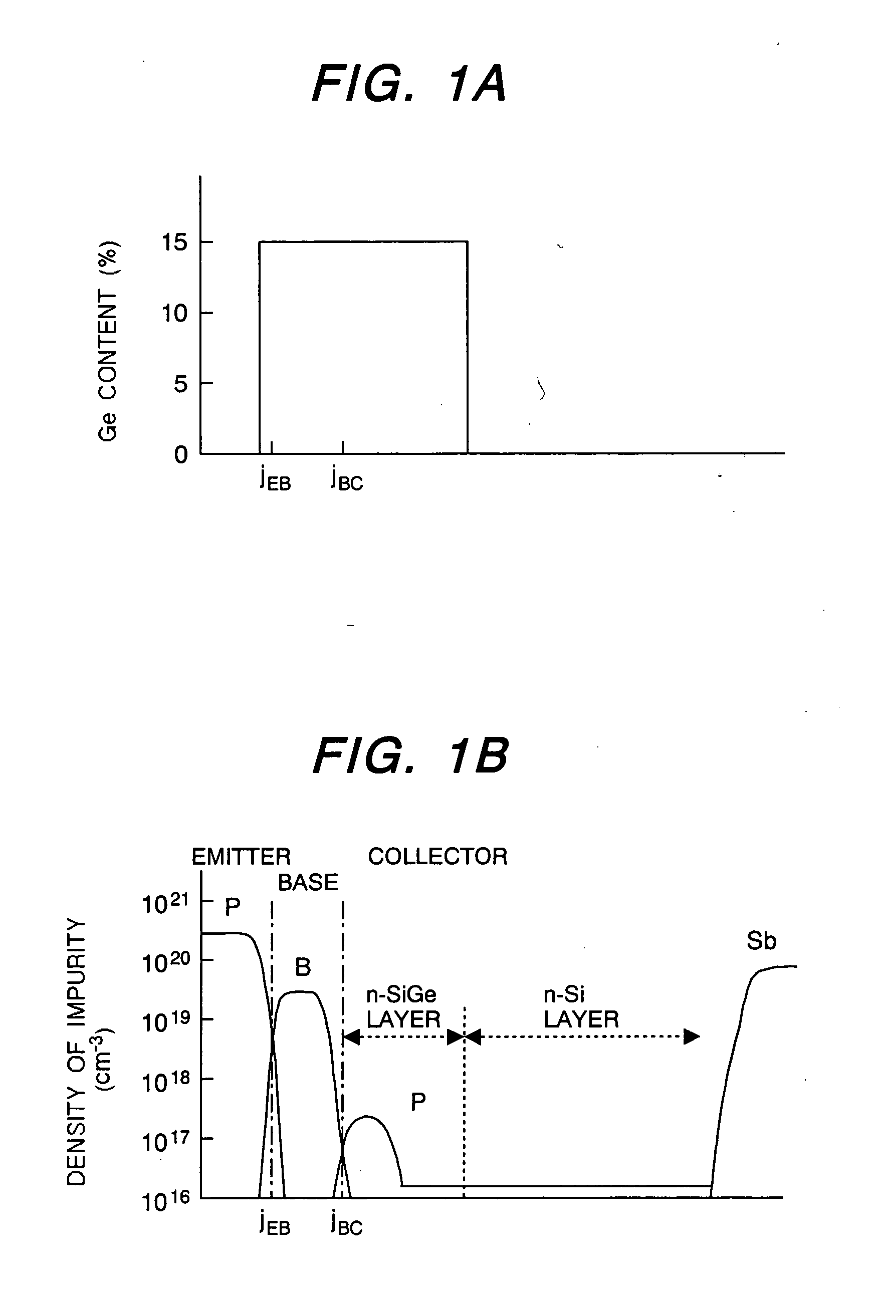
[0033]FIG. 1A and FIG. 1B illustrate the distribution of impurities (FIG. 1B) and germanium (FIG. 1A) in a principal portion of a semiconductor device according to a first embodiment of the present invention. The axes of abscissa in FIGS. 1A and 1B are shown in a correlated manner to facilitate understanding of a correlation between Ge distribution (Ge content) and impurity concentration (density of impurity). Silicon-germanium layer is distributed so as to cover a p-type base, and a heterointerface between silicon layer and silicon-germanium layer is disposed near the junction of n-type emitter and p-type base. A heterointerface on the collector side is disposed at a predetermined distance from the junction of n-type collector and p-type base, and a low concentration collector region is formed by two layers which are an n-type silicon-germanium layer and an n-type silicon layer. Phosphorus as n-impurity is distributed so as to have a peak near the collector-base junction in the n-t...

second embodiment

[0042]FIGS. 11A and 11B shows the distribution of germanium and the distribution of impurities, respectively, in a semiconductor device according to a second embodiment of the present invention. In this embodiment, the germanium composition in a silicon-germanium layer is set so as to decrease gradually from a certain position toward the boundary between it and an n-type silicon layer as shown in the figure. For example, in the case where the thickness of the n-type silicon-germanium layer is 30 to 40 nm, the germanium composition may be changed in the region of about 10 nm from the said boundary. The silicon-germanium layer having such a composition distribution does not have a steep heterointerface between it and the n-type silicon layer, thus diminishing the barrier itself which occurs in the conduction band as in FIG. 12. FIG. 12 shows a schematic band structure in the case of a steep Si / SiGe interface as indicated by dotted lines. In contrast therewith, the band structure indic...

third embodiment

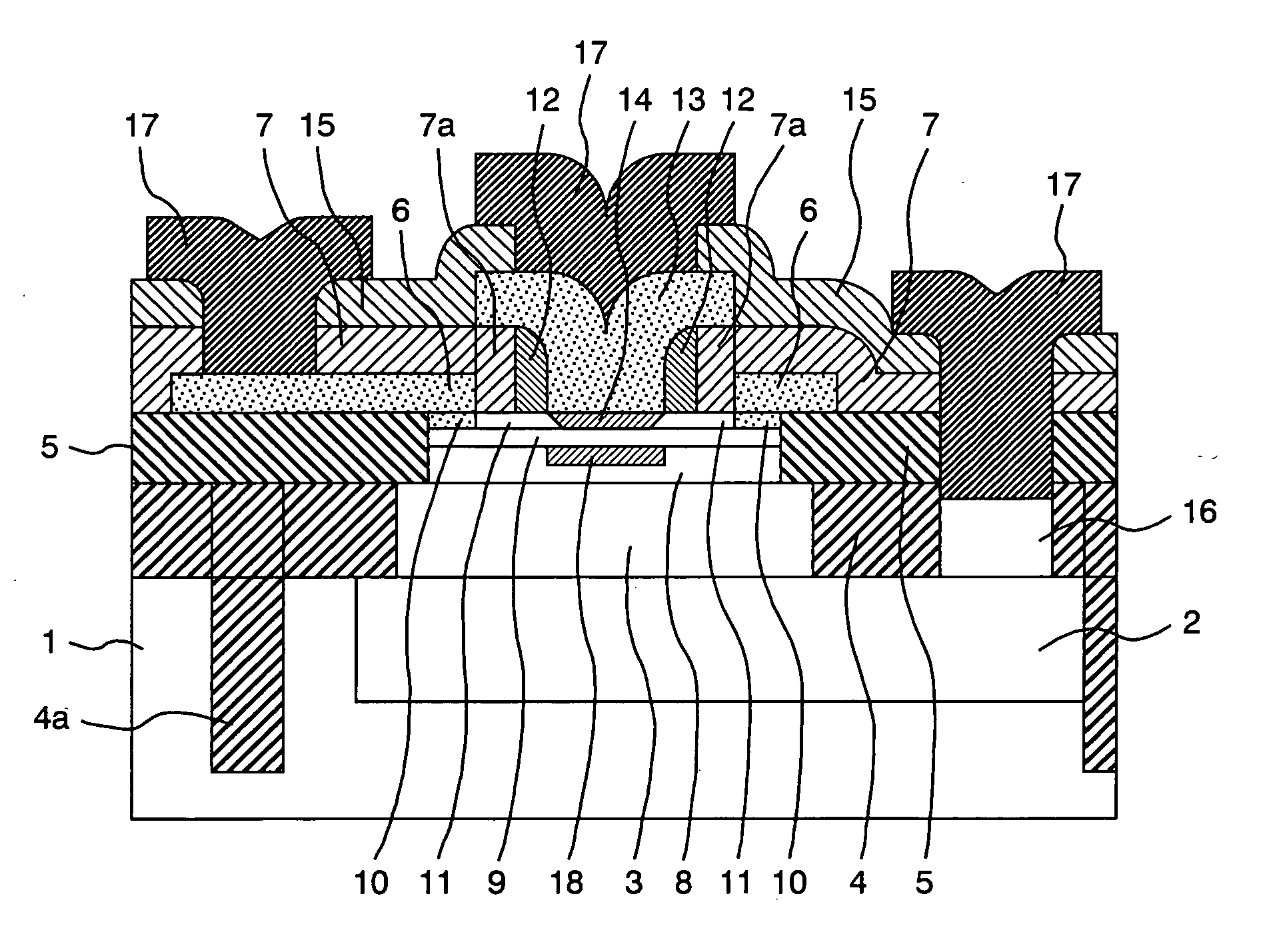
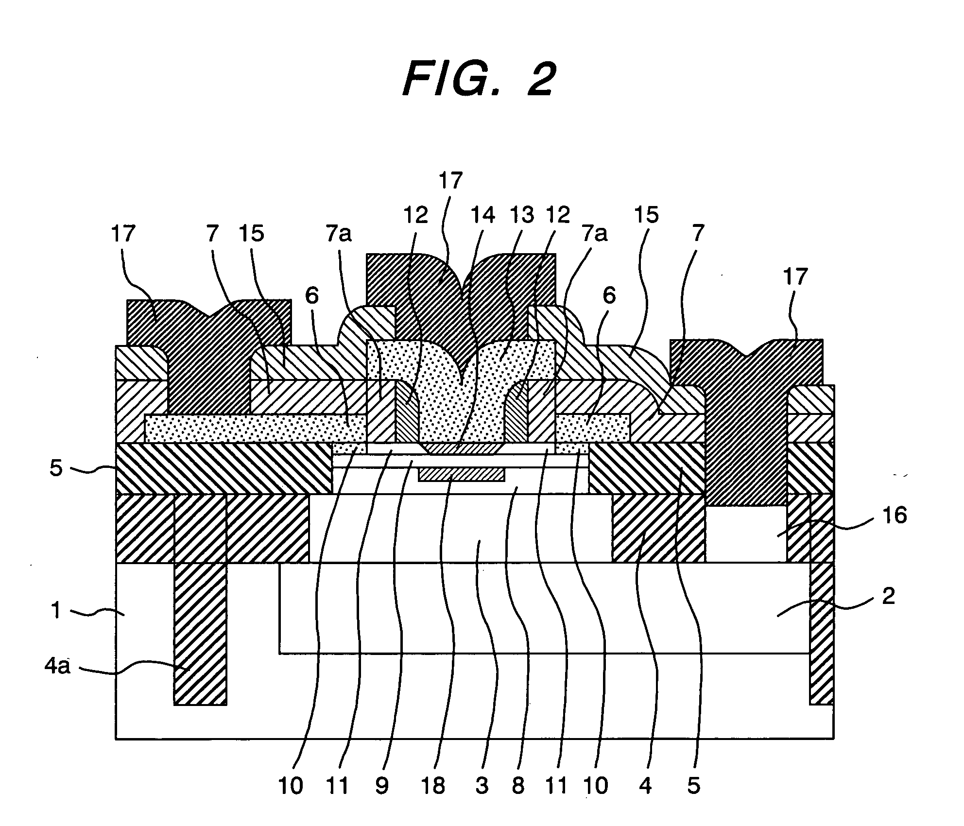
[0043]FIGS. 13 and 14 are respectively a sectional view of a semiconductor device according to a third embodiment of the present invention and a distribution diagram showing the distribution of impurities and germanium in a principal portion of the transistor. The axes of abscissa in FIGS. 14A and 14B are shown in a correlated manner to permit easier understanding of the correlation between Ge distribution and impurity concentration. Constituent portions shown in FIG. 13 are identified by the same reference numerals as in FIG. 2. The construction of a phosphorus doped region 18 in FIG. 13 is different from the construction shown in FIG. 2. This is a main different point. More specifically, in this embodiment, a peak value of phosphorus distribution is set so as to be positioned on the n-type silicon layer side with respect to the central part of the n-type silicon-germanium layer. By shifting the phosphorus distribution to the n-type silicon layer side, it is possible to hold the el...


PUM


Abstract

A bipolar type semiconductor device capable of attaining high current gain and high cut-off frequency and performing a satisfactory transistor operation also in a high current region while maintaining a high breakdown voltage performance, as well as a method of manufacturing the semiconductor device, are provided. In a collector comprising a first semiconductor layer and a second semiconductor layer narrower in band gap than the first semiconductor layer, an impurity is doped so as to have a peak of impurity concentration within the second collector layer and so that the value of the peak is higher than the impurity concentration at any position within the first collector layer. It is preferable to adjust the concentration of the doped impurity in such a manner that a collector-base depletion layer extends up to the first collector layer.

Description

CLAIM OF PRIORITY [0001] The present application claims priority from Japanese application JP 2004-251535 filed on Aug. 31, 2004, the content of which is hereby incorporated by reference into this application. BACKGROUND OF THE INVENTION [0002] 1. Field of the Invention [0003] The present invention relates to a semiconductor device, especially a bipolar transistor, and a method of manufacturing the same. [0004] 2. Description of the Prior Art [0005] Recently, bipolar transistors and integrated circuits with bipolar transistors mounted thereon have been utilized in various application fields. The bipolar transistor is advantageous over the field effect transistor in terms of high speed performance and high breakdown voltage performance, and its application is expanded for communication devices, storage systems, etc. Conventional examples of a bipolar transistor capable of attaining high speed and high breakdown voltage include a silicon-germanium heterobipolar transistor using the se...

Claims


Application Information

Patent Timeline
Patent Type & Authority Applications(United States)
IPC IPC(8): H01L31/109H01L21/331H01L29/732H01L29/737
CPCH01L29/0821H01L29/7378H01L29/66242
Inventor MIURA, MAKOTOWASHIO, KATSUYOSHISHIMAMOTO, HIROMI
Owner HITACHI LTD
Why Eureka
Try Eureka