
Lateral dmos device structure and manufacturing method thereof

A device, lateral technology, applied in the field of lateral DMOS devices and their manufacturing, can solve problems such as diode turn-off delay, and achieve the effect of improving operating speed, increasing yield, and preventing damage

Inactive Publication Date: 2010-06-02
DONGBU HITEK CO LTD
View PDF5 Cites 0 Cited by
  • Summary
  • Abstract
  • Description
  • Claims
  • Application Information

AI Technical Summary

Problems solved by technology

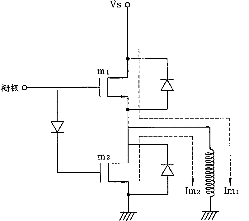
If a large current flows through the body diode, minority carrier accumulation, diode turn-off delay, and parasitic diode junction transistor operation may occur

Method used


Image

  • Lateral dmos device structure and manufacturing method thereof
  • Lateral dmos device structure and manufacturing method thereof
  • Lateral dmos device structure and manufacturing method thereof

Examples


Embodiment Construction

[0018] According to a specific embodiment, for regions other than the region where the protection diode is to be formed, the impurity region of the first conductivity type and the source region of the second conductivity type may be formed in the P-type body region. For the region where the protection diode is to be formed, only the first conductivity type impurity region is formed. In this way, for the region other than the region where the protection diode is to be formed, the body region of the first conductivity type and the well of the second conductivity type constitute a body diode, and for the region where the protection diode is to be formed, the body region of the first conductivity type and the well of the second conductivity type The conductivity type well constitutes a protection diode.

[0019] For example Figure 4 Illustrated and provided herein is the structure of a lateral DMOS device with a protection diode according to an embodiment. Hereinafter, a case w...


PUM


Abstract

A lateral DMOS device having a structure that prevents breakdown of a semiconductor device while enhancing the breakdown voltage property. The lateral DMOS device can include a body diode region having a second conduction type well region formed in a first conduction type semiconductor substrate, the second conduction type well region including a first conduction type body region and a drain region each formed in the second conduction type well region, a first conduction type impurity region formed in the first conduction type body region, a source region formed in the first conduction type body region, and a gate insulating film and a gate electrode formed on the first conduction type semiconductor substrate, wherein the first conduction type body region and the second conduction type well region compose a body diode; and a protective diode region in which the first conduction type impurity region is formed at a prescribed interval, wherein the first conduction type body region and the second conduction type well region compose a protective diode.

Description

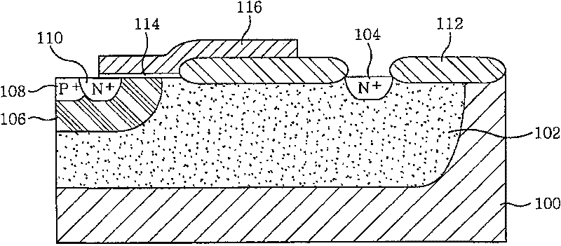
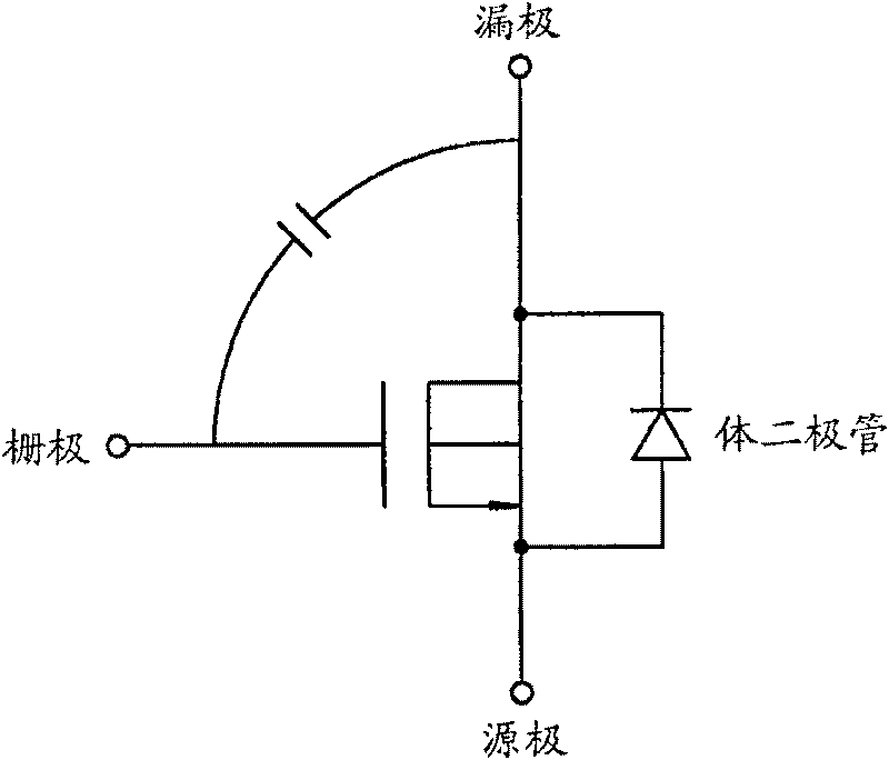
technical field [0001] This application claims priority from Korean Patent Application No. 10-2007-0048556 (filed May 18, 2007), the entire contents of which are hereby incorporated by reference. Background technique [0002] Power MOS field effect transistors (MOSFETs) can have higher input impedance than bipolar transistors. Therefore, the power MOSFET can have high power gain and simple gate drive circuit. In addition, since power MOSFETs are unipolar devices, there is no time delay due to minority carrier accumulation or recombination when the device is turned off. This power MOSFET can be used in switch-mode power supplies, lamp stabilization systems, and motor drive circuits. In general, semiconductor devices having a DMOS structure using planar diffusion technology are widely used. [0003] example figure 1 A lateral DMOS device is shown, which may include an N well 102 formed on and / or over a P-type semiconductor substrate 100 with a single concentration, and a d...

Claims


Application Information

Patent Timeline
Patent Type & Authority Patents(China)
IPC IPC(8): H01L21/336H01L29/78H01L29/06
CPCH01L29/1095H01L29/66681H01L29/7819H01L29/42368H01L29/0696
Inventor 方诚晚
Owner DONGBU HITEK CO LTD
Learn More